
Intel Celeron Processor in the 478-Pin Package at 1.80 GHz Datasheet


74 Datasheet
Intel
®
Celeron
®
Processor in the 478-Pin Package
D[63:0]#
Input/
Output
D[63:0]# (Data) are the data signals. These signals provide a 64-bit data path
between the processor system bus agents, and must connect the appropriate
pins on all such agents. The data driver asserts DRDY# to indicate a valid data
transfer.
D[63:0]# are quad-pumped signals and will thus be driven four times in a
common clock period. D[63:0]# are latched off the falling edge of both
DSTBP[3:0]# and DSTBN[3:0]#. Each group of 16 data signals correspond to a
pair of one DSTBP# and one DSTBN#.
The following are the groupings of the quad-pumped data signals, and their
associated data strobes and DBI#:
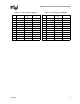
Data Group DSTBN# / DSTBP# DBI#
D[15:0]# 0 0
D[31:16]# 1 1
D[47:32]# 2 2
D[63:48]# 3 3
Furthermore, the DBI# pins determine the polarity of the data signals. Each group
of 16 data signals corresponds to one DBI# signal. When the DBI# signal is
active, the corresponding data group is inverted and therefore sampled active
high.
DBI[3:0]#
Input/
Output
DBI[3:0]# are source synchronous and indicate the polarity of the D[63:0]#
signals. The DBI[3:0]# signals are activated when the data on the data bus is
inverted. The bus agent will invert the data bus signals if more than half the bits,
within the covered group, would change level in the next cycle.
The following are the DBI[3:0] assignments to the data bus:
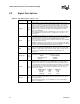
Bus Signal Data Bus Signals
DBI3# D[63:48]#
DBI2# D[47:32]#
DBI1# D[31:16]#
DBI0# D[15:0]#
DBR# Output
DBR# is used only in processor systems where no debug port is implemented on
the system board. DBR# is used by a debug port interposer so that an in-target
probe can drive system reset. If a debug port is implemented in the system,
DBR# is a no connect in the system. DBR# is not a processor signal.
DBSY#
Input/
Output
DBSY# (Data Bus Busy) is asserted by the agent responsible for driving data on
the processor system bus to indicate that the data bus is in use. The data bus is
released after DBSY# is deasserted. This signal must connect the appropriate
pins on all processor system bus agents.
DEFER# Input
DEFER# is asserted by an agent to indicate that a transaction cannot be
guaranteed in-order completion. Assertion of DEFER# is normally the
responsibility of the addressed memory or Input/Output agent. This signal must
connect the appropriate pins of all processor system bus agents.
DP[3:0]#
Input/
Output
DP[3:0]# (Data parity) provide parity protection for the D[63:0]# signals. They are
driven by the agent responsible for driving D[63:0]#, and must connect the
appropriate pins of all Celeron processor in the 478-pin package system bus
agents.
DRDY#
Input/
Output
DRDY# (Data Ready) is asserted by the data driver on each data transfer,
indicating valid data on the data bus. In a multi-common clock data transfer,
DRDY# may be deasserted to insert idle clocks. This signal must connect the
appropriate pins of all processor system bus agents.
DSTBN[3:0]#
Input/
Output
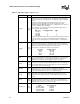
The following are the DSTBN data strobes that are used to latch D[63:0]#:
Signals Associated Strobe
D[15:0]#, DBI0# DSTBN0#
D[31:16]#, DBI1# DSTBN1#
D[47:32]#, DBI2# DSTBN2#
D[63:48]#, DBI3# DSTBN3#
Table 32. Signal Description (Sheet 3 of 7)
Name Type Description