
Intel Celeron Processor in the 478-Pin Package at 1.80 GHz Datasheet


Datasheet 19
Intel
®
Celeron
®
Processor in the 478-Pin Package
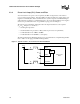
2.5 System Bus Signal Groups
To simplify the following discussion, the system bus signals have been combined into groups by
buffer type. AGTL+ input signals have differential input buffers, which use GTLREF as a reference
level. In this document, the term AGTL+ Input refers to the AGTL+ input group as well as the
AGTL+ I/O group when receiving. Similarly, AGTL+ Output refers to the AGTL+ output group as
well as the AGTL+ I/O group when driving.
With the implementation of a source synchronous data bus comes the need to specify two sets of
timing parameters. One set is for common clock signals which are dependent upon the rising edge
of BCLK0 (ADS#, HIT#, HITM#, etc.) and the second set is for the source synchronous signals
which are relative to their respective strobe lines (data and address) as well as the rising edge of
BCLK0. Asychronous signals are still present (A20M#, IGNNE#, etc.) and can become active at
any time during the clock cycle. Table 3 identifies which signals are common clock, source
synchronous, and asynchronous.
NOTE:
1. Refer to Chapter 5.0 for signal descriptions.
2. These AGTL+ signals do not have on-die termination and must be terminated on the system board.
3. In processor systems where there is no debug port implemented on the system board, these signals are used
to support a debug port interposer. In systems with the debug port implemented on the system board, these
signals are no connects.
4. These signal groups are not terminated by the processor. Refer to Section 2.4 and the ITP700 Debug Port
Design Guide, and the appropriate Platform Design Guide as referenced in Table 1 for termination
requirements and further details.
5. The value of these pins during the active-to-inactive edge of RESET# determine processor configuration
options. See Section 7.1 for details.
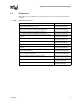
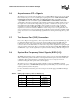
Table 3. System Bus Pin Groups
Signal Group Type Signals
1
AGTL+ Common Clock Input
Synchronous
to BCLK[1:0]
BPRI#, DEFER#, RESET#
2
, RS[2:0]#, RSP#, TRDY#
AGTL+ Common Clock I/O
Synchronous
to BCLK[1:0]
AP[1:0]#, ADS#, BINIT#, BNR#, BPM[5:0]#
2
, BR0#
2
,
DBSY#, DP[3:0]#, DRDY#, HIT#, HITM#, LOCK#,
MCERR#
AGTL+ Strobes
Synchronous
to BCLK[1:0]
ADSTB[1:0]#, DSTBP[3:0]#, DSTBN[3:0]#
AGTL+ Source Synchronous I/O
Synchronous
to assoc.
strobe
Signal Associated Strobe
REQ[4:0]#, A[16:3]#
5
ADSTB0#
A[35:17]#
5
ADSTB1#
D[15:0]#, DBI0# DSTBP0#, DSTBN0#
D[31:16]#, DBI1# DSTBP1#, DSTBN1#
D[47:32]#, DBI2# DSTBP2#, DSTBN2#
D[63:48]#, DBI3# DSTBP3#, DSTBN3#
Asynchronous GTL+ Input
4, 5
A20M#, IGNNE#, INIT#, LINT0/INTR, LINT1/NMI, SMI#,
SLP#, STPCLK#
Asynchronous GTL+ Output
4
FERR#, IERR#, THERMTRIP#, PROCHOT#
TAP Input
4
Synchronous
to TCK
TCK, TDI, TMS, TRST#
TAP Output
4
Synchronous
to TCK
TDO
System Bus Clock Clock BCLK[1:0], ITP_CLK[1:0]
3
Power/Other
V
CC, VCCA, VCCIOPLL, VID[4:0], VSS, VSSA, GTLREF[3:0],
COMP[1:0], RESERVED, TESTHI[12:8], TESTHI[5:0],
THERMDA, THERMDC, VCC_SENSE, VSS_SENSE,
VCCVID, BSEL[1:0], SKTOCC#, DBR#
3
,
ITPCLKOUT[1:0], PWRGOOD