
Guide

Mobile Intel Pentium 4 Processor–M and Mobile Intel Celeron Processor FSB Design Guidelines
R
Intel
®
852GM Chipset Platform Design Guide 41
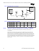
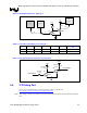
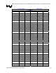
Figure 11. Routing Illustration for Topology 1B
VCCP
Rtt
CPU
ICH4-M
(or sys. receiver)
L1
L2
L3
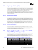
Table 6. Layout Recommendations for Topology 1B
L1 L2 L3 Rtt Transmission Line Type
0.5” – 12.0” 0” – 3.0” 0” – 3.0” 56 Ω ± 5% Micro-strip
0.5” – 12.0” 0” – 3.0” 0” – 3.0” 56 Ω ± 5% Strip-line
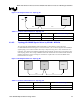
4.3.4.3. Topology 1C: Open Drain (OD) Signals Driven by the Processor –
PROCHOT#
The Topology 1C OD signal PROCHOT#, should adhere to the following routing and layout
recommendations. Table 7 lists the recommended routing requirements for the PROCHOT# signal. The
routing guidelines allow the signal to be routed as either a micro-strip or strip-line using 55 Ω ± 15%
characteristic trace impedance. Figure 12 shows the recommended implementation for providing voltage
translation between the processor’s PROCHOT# signal and a system receiver that utilizes a 3.3-V
interface voltage (shown as VCCP).
Series resistor Rs is a component of the voltage translation logic and serves as a driver isolation resistor.
Rs is shown separated by distance L3 from the first bipolar junction transistor (BJT), Q1, to emphasize
the placement of Rs with respect to Q1. The placement of Rs a distance L3 before the Q1 BJT is a
specific implementation of the generalized voltage translator circuit shown in Figure 17. Rs should be
placed at the beginning of the T-split from the PROCHOT# signal. The pull-up voltage for termination
resistor Rtt is VCCP.
Intel recommends that PROCHOT# be routed using the voltage translation logic shown in Figure 12.