
Guide

Mobile Intel Pentium 4 Processor–M and Mobile Intel Celeron Processor FSB Design Guidelines
R
34 Intel
®
852GM Chipset Platform Design Guide
4.3.1. Source Synchronous (SS) Signal Group
Source synchronous groups and associated strobes should be routed on the same layer for the entire
length of the bus. This results in a significant reduction of the flight time skew since the dielectric
thickness, line width, and velocity of the signals will be uniform across a single layer of the stackup.
There is no guarantee of a relationship of dielectric thickness, line width, and velocity between layers.
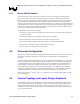
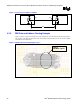
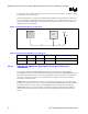
Figure 4. Processor Topology
GMCH
Processor
Length L1
Package trace
Motherboard PCB trace
Pad
Pad
4.3.1.1. Source Synchronous Data Group
Data signals of the same source synchronous group should be routed to the same pad-to-pad length
within ± 0.100 of the associated strobes (within the min & max of both strobe). As a result, additional
trace will be added to some data nets on the system board in order for all trace lengths within the same
data group to be the same length (± 0.100 inches) from the pad of the processor to the associated pad
of the chipset.
A data strobe and its complement should be routed to a length equal to their corresponding data group's
mean pad-to-pad length ± 0.025 inches.
Equation 1. Calculation to Determine Package Delta Addition to Motherboard Length for UP
Systems
)cs_pkglen(cs_pkglen)cpu_pkglenn(cpu_pkgledelta
strobenet*strobenetnet,strobe
−
+
−
=
Refer to the Intel
®
852GM Chipset GMCH Datasheet for GMCH package dimensions and refer to the
Mobile Intel
®
Pentium
®
4 Processor–M Datasheet for package dimensions.
Note: * Strobe package length is the average of the strobe pair.