
Guide

System Memory Design Guidelines (DDR-SDRAM)
R
Intel
®
852GM Chipset Platform Design Guide 121
7.3.7. CPC Signals – SMA[5,4,2,1], SMAB[5,4,2,1]
The Intel 852GM GMCH chipset control signals, SCKE[3:0] and SCS#[3:0], are common clocked
signals. They are “clocked” into the DDR SDRAM devices using clock signals SCK/SCK#[5:0]. The
GMCH drives the CPC and clock signals together, with the clocks crossing in the valid control window.
The GMCH provides one set of CPC signals per SO-DIMM slot.
Refer to Table 38 for the CKE and CS# signal to SO-DIMM mapping.
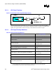
Table 45. CPC Signal to SO-DIMM Mapping
Signal Relative To SO-DIMM Pin
SMA[1] SO-DIMM0 AD14
SMA[2] SO-DIMM0 AD13
SMA[4] SO-DIMM0 AD11
SMA[5] SO-DIMM0 AC13
SMAB[1] SO-DIMM1 AD16
SMAB[2] SO-DIMM1 AC12
SMAB[4] SO-DIMM1 AF11
SMAB[5] SO-DIMM1 AD10
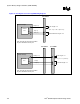
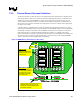
• The CPC signal routing should transition from an external layer to an internal signal layer under the
GMCH.
• Keep to the same internal layer until transitioning back out to an external layer to connect to the
appropriate pad of the SO-DIMM connector and the parallel termination resistor.
• If the layout requires additional routing before the termination resistor, return to the same internal
layer and transition back out to an external layer immediately prior to parallel termination resistor.
• External trace lengths should be minimized. Intel suggests that the parallel termination be placed on
both sides of the board to simplify routing and minimize trace lengths.
• All internal and external signals should be ground reference to keep the path of return current
continuous. Intel suggests that all control signals be routed on the same internal layer.
• Resistor packs are acceptable for the parallel (Rt) control termination resistors, but control signals
can’t be placed within the same R pack as the data or command signals. Figure 60 and Table 46
below depict the recommended topology and layout routing guidelines for the DDR-SDRAM
control signals.