
Guide

Intel Celeron M Processor Front Side Bus Design Guidelines
R
Intel
®
852GM Chipset Platform Design Guide 79
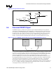
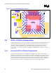
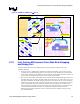
Figure 41. COMP2 & COMP0 27.4-Ω Traces
PRIMARY SIDE
SECONDARY SIDE
SECONDARY SIDE
COMP0
COMP2
18
-mil Dog Bone
18
-
mil Trace
27.4
Ω
1%
27.4
Ω
1%
COMP1
COMP3
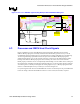
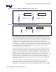
PRIMARY SIDE
SECONDARY SIDE
COMP0
COMP2
18-mil Trace
18
-
mil Trace
27.4
Ω
1%
27.4
Ω
1%
COMP0
COMP2COMP2
5.10. Intel Celeron M Processor Front Side Bus Strapping
and Debug Port
The Intel Celeron M Processor and GMCH both have pins that require termination for proper
component operation.
1. For the processor, a stuffing option should be provided for the TEST[3:1] pin to allow a 1 kΩ ±
5% pull-down to ground for testing purposes. For proper processor operation, the resistor should
not be stuffed. Resistors for the stuffing option on these pins should be placed within 2.0 inches of
the processor. For normal operation, these resistors should not be stuffed.
2. The processor’s ITP signals, TDI, TMS, TRST, and TCK should assume default logic values even
if the ITP debug port is not used. The TDO signal may be left open or no connect in this case. The
table below summarizes the default strapping resistors for these signals. These resistors should be
connected to the processor within 2.0 inches from their respective pins. It is important to note that
Table 29 is applicable only when neither the onboard ITP nor ITP interposer are planned to be
used. Intel does not recommend use of the ITP interposer debug port if there is a dependence only
on the motherboard termination resistors. The signals below should be isolated from the
motherboard via specific termination resistors on the ITP interposer itself per interposer debug
port recommendations.