
Intel Celeron Processor in the 478-Pin Package at 1.80 GHz Datasheet

40 Datasheet
Intel
®
Celeron
®
Processor in the 478-Pin Package
3.2 System Bus Signal Quality Specifications and
Measurement Guidelines
Many scenarios have been simulated to generate a set of AGTL+ layout guidelines that are
available in the Platform Design Guidelines.
Table 20 provides the signal quality specifications for all processor signals for use in simulating
signal quality at the processor silicon.
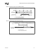
The Celeron processor in the 478-pin package
maximum allowable overshoot and undershoot
specifications for a given duration of time are detailed in Table 22 through Table 25. Figure 17
shows the system bus ringback tolerance for low-to-high transitions and Figure 18 shows ringback
tolerance for high-to-low transitions.
NOTES:
1. All signal integrity specifications are measured at the processor silicon.
2. Unless otherwise noted, all specifications in this table apply to all Celeron processor in the 478-pin package
frequencies and cache sizes.
3. Specifications are for the edge rate of 0.3 – 4.0 V/ns.
4. All values specified by design characterization.
5. Ringback between GTLREF + 100 mV and GTLREF
– 100 mV is not supported.
6. Intel recommends simulations not exceed a ringback value of GTLREF
± 200 mV to allow margin for other
sources of system noise.
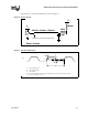
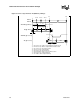
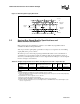
Figure 16. BCLK Signal Integrity Waveform
Crossing
Voltage
Threshold
Region
VH
VL
Overshoot
Undershoot
Ringback
Margin
Rising Edge
Ringback
Falling Edge
Ringback,
BCLK0
BCLK1
Crossing
Voltage
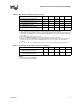
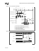
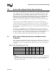
Table 20. Ringback Specifications for AGTL+ and Asynchronous GTL+ Signal Groups
Signal Group Transition
Maximum Ringback
(with Input Diodes Present)
Unit Figure Notes
All Signals 0
→ 1 GTLREF + 0.100 V 17 1,2,3,4,5,6,7
All Signals 1
→ 0 GTLREF - 0.100 V 18 1,2,3,4,5,6,7