
Intel Celeron Processor on 0.13 Micron Process in the 478-Pin Package Datasheet

Intel
®
Celeron
®
Processor on 0.13 Micron Process in the 478-Pin Package Datasheet 25
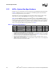
Electrical Specifications
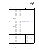
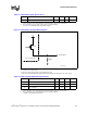
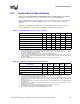
Table 9. System Bus Differential BCLK Specifications
Symbol Parameter Min Typ Max Unit Fig Notes
1
NOTES:
1. Unless otherwise noted, all specifications in this table apply to all processor frequencies.
V
L
Input Low Voltage –0.150 0.000 N/A V 8
V
H
Input High Voltage 0.660 0.710 0.850 V 8
V
CROSS(abs)
Absolute Crossing
Point
0.250 N/A 0.550 V 8, 9
2, 3,
4
2. Crossing voltage is defined as the instantaneous voltage value when the rising edge of BCLK0 equals the
falling edge of BCLK1.
3. V
Havg
is the statistical average of the V
H
measured by the oscilloscope.
4. The crossing point must meet the absolute and relative crossing point specifications simultaneously.
V
CROSS(rel)
Relative Crossing
Point
0.250 +
0.5(V
Havg
–0.710)
N/A
0.550 +
0.5(V
Havg
–0.710)
V 8, 9
2,
3,
4,
5
5. V
Havg
can be measured directly using “Vtop” on Agilent scopes and “High” on Tektronix scopes.
∆V
CROSS
Range of Crossing
Points
N/A N/A 0.140 V 8, 9
2,
6
6. ∆V
CROSS
is defined as the total variation of all crossing voltages as defined in note 2.
V
OV
Overshoot N/A N/A V
H
+ 0.3 V 8
7
7. Overshoot is defined as the absolute value of the maximum voltage.
V
US
Undershoot –0.300 N/A N/A V 8
8
8. Undershoot is defined as the absolute value of the minimum voltage.
V
RBM
Ringback Margin 0.200 N/A N/A V 8
9
9. Ringback Margin is defined as the absolute voltage difference between the maximum Rising Edge Ringback
and the maximum Falling Edge Ringback.
V
TM
Threshold Margin V
CROSS
– 0.100 N/A V
CROSS
+ 0.100 V 8
10
10. Threshold Region is defined as a region entered around the crossing point voltage in which the differential
receiver switches. It includes input threshold hysteresis.
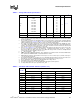
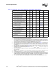
Table 10. AGTL+ Signal Group DC Specifications
Symbol Parameter Min Max Unit Notes
1
NOTES:
1. Unless otherwise noted, all specifications in this table apply to all processor frequencies.
GTLREF Reference Voltage 2/3 VCC – 2% 2/3 VCC + 2% V
V
IH
Input High Voltage 1.10*GTLREF VCC V
2,
3
2. VIL is defined as the maximum voltage level at a receiving agent that will be interpreted as a logical low value.
3. The VCC referred to in these specifications is the instantaneous VCC.
V
IL
Input Low Voltage 0.0 0.9*GTLREF V
3,
4,
5
4. VIH is defined as the minimum voltage level at a receiving agent that will be interpreted as a logical high
value.
5. VIH and VOH may experience excursions above VCC. However, input signal drivers must comply with the
signal quality specifications in this chapter.
V
OH
Output High Voltage N/A VCC V
6
6. Vol max of 0.450 V is guaranteed when driving into a test load of 50 Ω as indicated in Figure 6.
I
OL
Output Low Current N/A 50 mA
3
I
HI
Pin Leakage High N/A 100 µA
7
7. Leakage to VSS with pin held at VCC.
I
LO
Pin Leakage Low N/A 500 µA
8
8. Leakage to VCC with Pin held at 300 mV.
R
ON
Buffer On Resistance 7 11 Ω
9
9. Refer to processor I/O Buffer Models for I/V characteristics.