
Intel Celeron Processor on 0.13 Micron Process in the 478-Pin Package Datasheet

26 Intel
®
Celeron
®
Processor on 0.13 Micron Process in the 478-Pin Package Datasheet
Electrical Specifications
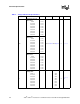
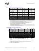
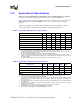
Table 11. Asynchronous GTL+ Signal Group DC Specifications
Symbol Parameter Min Max Unit Notes
1
NOTES:
1. Unless otherwise noted, all specifications in this table apply to all processor frequencies.
V
IH
Input High Voltage Asynch GTL+ 1.10*GTLREF VCC V
2,
3,
4
2. VIH and VOH may experience excursions above VCC. However, input signal drivers must comply with the
signal quality specifications in
Chapter 3, “System Bus Signal Quality Specifications”.
3. The VCC referred to in these specifications refers to instantaneous VCC.
4. This specification applies to the asynchronous GTL+ signal group.
V
IL
Input Low Voltage Asynch. GTL+ 0 0.9*GTLREF V
4
V
OH
Output High Voltage N/A VCC V
2,
3, 5
5. All outputs are open-drain.
I
OL
Output Low Current N/A 50 mA
6,
7
6. The maximum output current is based on maximum current handling capability of the buffer and is not spec-
ified into the test load shown in Figure 6.
7. VOL max of 0.270 V is guaranteed when driving into a test load of 50 Ω as indicated in Figure 6 for the Asyn-
chronous GTL+ signals.
I
HI
Pin Leakage High N/A 100 µA
8
8. Leakage to VSS with pin held at VCC.
I
LO
Pin Leakage Low N/A 500 µA
9
9. Leakage to VCC with pin held at 300 mV.
R
on
Buffer On Resistance Asynch GTL+ 7 11 Ω
4,
10
10. Refer to the processor I/O Buffer Models for I/V characteristics.
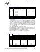
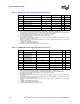
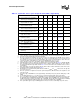
Table 12. PWRGOOD and TAP Signal Group DC Specifications
Symbol Parameter Min Max Unit Notes
1
NOTES:
1. Unless otherwise noted, all specifications in this table apply to all processor frequencies.
V
HYS
Input Hysteresis 200 300 mV
2
2. V
HYS
represents the amount of hysteresis, nominally centered about 1/2 VCC for all TAP inputs.
V
T+
Input Low to High
Threshold Voltage
1/2*(VCC + VHYS_MIN) 1/2*(VCC + VHYS_MAX) V
3
3. The VCC referred to in these specifications refers to instantaneous VCC.
V
T-
Input High to Low
Threshold Voltage
1/2*(VCC – VHYS_MAX) 1/2*(VCC – VHYS_MIN) V
3
V
OH
Output High Voltage N/A VCC V
3,
4,
5
4. All outputs are open-drain.
5. The TAP signal group must comply with the signal quality specifications in Chapter 3, “System Bus Signal Quality
Specifications”
.
I
OL
Output Low Current N/A 40 mA
6,
7
6. The maximum output current is based on maximum current handling capability of the buffer and is not spec-
ified into the test load shown in
Figure 6.
7. Vol max of 0.320 V is guaranteed when driving into a test load of 50 Ω as indicated in Figure 6 for the TAP
signals.
I
HI
Pin Leakage High N/A 100 µA
8
8. Leakage to VSS with pin held at VCC.
I
LO
Pin Leakage Low N/A 500 µA
9
9. Leakage to VCC with pin held at 300 mV
R
ON
Buffer On Resistance 8.75 13.75 Ω
10
10. Refer to I/O Buffer Models for I/V characteristics.