
Intel Celeron Processor in the 478-Pin Package at 1.80 GHz Datasheet

72 Datasheet
Intel
®
Celeron
®
Processor in the 478-Pin Package
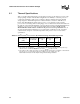
5.2 Signal Descriptions
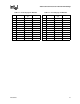
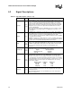
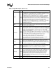
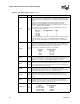
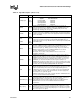
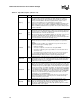
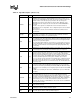
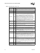
Table 32. Signal Description (Sheet 1 of 7)
Name Type Description
A[35:3]#
Input/
Output
A[35:3]# (Address) define a 2
36
-byte physical memory address space. In sub-
phase 1 of the address phase, these pins transmit the address of a transaction. In
sub-phase 2, these pins transmit transaction type information. These signals
must connect the appropriate pins of all agents on the Celeron processor in the
478-pin package system bus. A[35:3]# are protected by parity signals AP[1:0]#.
A[35:3]# are source synchronous signals and are latched into the receiving
buffers by ADSTB[1:0]#.
On the active-to-inactive transition of RESET#, the processor samples a subset
of the A[35:3]# pins to determine power-on configuration. See Section 7.1 for
more details.
A20M# Input
If A20M# (Address-20 Mask) is asserted, the processor masks physical address
bit 20 (A20#) before looking up a line in any internal cache and before driving a
read/write transaction on the bus. Asserting A20M# emulates the 8086
processor’s address wrap-around at the 1-Mbyte boundary. Assertion of A20M#
is only supported in real mode.
A20M# is an asynchronous signal. However, to ensure recognition of this signal
following an Input/Output write instruction, it must be valid along with the TRDY#
assertion of the corresponding Input/Output Write bus transaction.
ADS#
Input/
Output
ADS# (Address Strobe) is asserted to indicate the validity of the transaction
address on the A[35:3]# and REQ[4:0]# pins. All bus agents observe the ADS#
activation to begin parity checking, protocol checking, address decode, internal
snoop, or deferred reply ID match operations associated with the new
transaction.
ADSTB[1:0]#
Input/
Output
Address strobes are used to latch A[35:3]# and REQ[4:0]# on their rising and
falling edges. Strobes are associated with signals as follows:
Signal Associated Strobe
REQ[4:0]#, A[16:3]# ADSTB0#
A[35:17]# ADSTB1#
AP[1:0]#
Input/
Output
AP[1:0]# (Address Parity) are driven by the request initiator along with ADS#,
A[35:3]#, and the transaction type on the REQ[4:0]#. A correct parity signal is
high if an even number of covered signals are low and low if an odd number of
covered signals are low. This allows parity to be high when all the covered signals
are high. AP[1:0]# should connect the appropriate pins of all Celeron processor in
the 478-pin package system bus agents. The following defines the coverage
model of these signals:
Request Signal Subphase Subphase 2
A[35:24]# AP0# AP1#
A[23:3]# AP1# AP0#
REQ[4:0]# AP1# AP0#
BCLK[1:0] Input
The differential pair BCLK (Bus Clock) determines the system bus frequency. All
processor system bus agents must receive these signals to drive their outputs
and latch their inputs.
All external timing parameters are specified with respect to the rising edge of
BCLK0 crossing V
CROSS
.