
Guide

System Memory Design Guidelines (DDR-SDRAM)
R
96 Intel
®
852GM Chipset Platform Design Guide
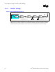
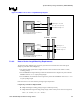
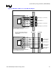
Length matching is not required from the SO-DIMM1 to the parallel termination resistors. Figure 48 on
the following page depicts the length matching requirements between the SDQ, SDM, and SDQS
signals within a byte lane. Byte lane mapping is defined in Table 36 below.
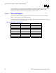
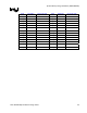
7.3.4.4. SDQ to SDQS Mapping
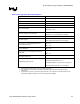
Table 36 below defines the mapping between the nine byte lanes, nine mask bits, and the nine SDQS
signals, as required to do the required length matching.
The following signals are should not be routed out SDQ[71:64], SDM[8], and SDQS[8] as these signals
are not supported in the Intel 852GM chipset.
Table 36. SDQ/SDM to SDQS Mapping
Signal Mask Relative To
SDQ[7:0] SDM[0] SDQS[0]
SDQ[15:8] SDM[1] SDQS[1]
SDQ[23:16] SDM[2] SDQS[2]
SDQ[31:24] SDM[3] SDQS[3]
SDQ[39:32] SDM[4] SDQS[4]
SDQ[56:40] SDM[5] SDQS[5]
SDQ[55:48] SDM[6] SDQS[6]
SDQ[63:56] SDM[7] SDQS[7]