
Guide

System Memory Design Guidelines (DDR-SDRAM)
R
92 Intel
®
852GM Chipset Platform Design Guide
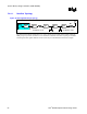
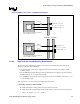
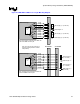
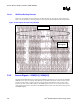
7.3.4.1. Data Bus Topology
Figure 46. Data Signal Routing Topology
Rt
SO-DIMM1 PAD
SO-DIMM0 PAD
Vtt
P1
L1
GMCH
Die
GMCH
L2 L3
L4
The data signals should be routed using a 2 to 1 trace spacing to trace width ratio for signals within the
DDR group, except clocks and strobes. There should be a minimum of 20 mils of spacing to non-DDR
related signals. Data signals should be routed on inner layers with minimized external trace lengths.