
Guide

Mobile Intel Pentium 4 Processor–M and Mobile Intel Celeron Processor FSB Design Guidelines
R
46 Intel
®
852GM Chipset Platform Design Guide
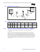
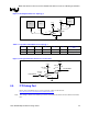
4.4.1. Logic Analyzer Interface (LAI)
Intel is working with two logic analyzer vendors to provide logic analyzer interfaces (LAIs) for use in
debugging the Mobile Intel Pentium 4 Processor–M based system. Tektronix* and Agilent* should be
contacted to get specific information about their logic analyzer interfaces. The following information is
general in nature. Specific information must be obtained from the logic analyzer vendor.
Due to the complexity of the Mobile Intel Pentium 4 Processor–M based system, the LAI is critical in
providing the ability to probe and capture Front Side Bus signals. There are two sets of considerations to
keep in mind when designing a Mobile Intel Pentium 4 Processor–M that can make use of an LAI:
mechanical and electrical.
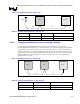
4.4.1.1. Mechanical Considerations
The LAI is installed between the processor socket and the Mobile Intel Pentium 4 Processor–M. The
LAI pins plug into the socket, while the Mobile Intel Pentium 4 Processor–M plugs into a socket on the
LAI. Cabling that is part of the LAI egresses the system to allow an electrical connection between the
Mobile Intel Pentium 4 Processor–M and a logic analyzer. The maximum volume occupied by the LAI,
known as the keepout volume, as well as the cable egress restrictions, should be obtained from the logic
analyzer vendor. System designers must make sure that the keepout volume remains unobstructed inside
the system. Note that it is possible that the keepout volume reserved for the LAI may include space
normally occupied by the Mobile Intel Pentium 4 Processor–M heat sink. If this is the case, the logic
analyzer vendor will provide a cooling solution as part of the LAI.
4.4.1.2. Electrical Considerations
The LAI will also affect the electrical performance of the Front Side Bus; therefore, it is critical to
obtain electrical load models from each of the logic analyzers in order to run system level simulations to
prove that their tool will work in the system. Contact the logic analyzer vendor for electrical
specifications and load models for the LAI solution they provide.
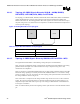
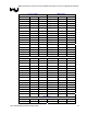
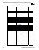
4.5. Mobile Intel Pentium 4 Processor–M and Intel 852GM
Chipset FSB Signal Package Lengths
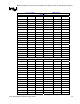
Table 12 lists the preliminary package trace lengths of the Mobile Intel Pentium 4 Processor–M and the
Intel 852GM GMCH for the source synchronous data and address signals. Refer to Section 4.3.1 for
further details. The Mobile Intel Pentium 4 Processor–M and Intel 852GM GMCH package traces are
routed as micro-strip lines with a nominal characteristic impedance of 55 Ω ± 15%.
Table 12. Mobile Intel Pentium 4 Processor-M and Intel 852GM Chipset Package Lengths
Processor lengths GMCH Lengths
Signal Processor
Ball
Length
(inches)
Signal GMCH ball Length
(mils)
Address Group 0
ADSTB[0]# L5 0.210 HADSTB[0]# T26 419
A[3]# K2 0.368 HA[3]# P23 468
A[4]# K4 0.265 HA[4]# T25 353