
Guide

Mobile Intel Pentium 4 Processor–M and Mobile Intel Celeron Processor FSB Design Guidelines
R
Intel
®
852GM Chipset Platform Design Guide 43
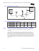
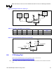
Figure 13. Routing Illustration for Topology 2A
CPU
ICH4-M
VCCP
L2
Rtt
L1
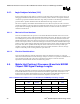
Table 8. Layout Recommendations for Topology 2A
L1
L2 Rtt Transmission Line Type
0.5” – 12.0” 0” – 3.0” 300 Ω ± 5% Micro-strip
0.5” – 12.0” 0” – 3.0” 300 Ω ± 5% Strip-line
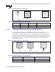
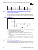
4.3.4.5. Topology 2B: CMOS Signals Driven by ICH4-M – DPSLP#
The Topology 2B CMOS DPSLP# signal should adhere to the following routing and layout
recommendations illustrated in Figure 14. As listed in Table 9, the L1 and L2 segments of the DPSLP#
signal topology can be routed as either micro-strip or strip-lines using 55 Ω ± 15% characteristic trace
impedance. Note that the Intel ICH4-M’s DPSLP# signal should be routed point-to-point with the daisy
chain topology shown. The routing of DPSLP# at the CPU should fork out to both the ICH4-M and the
GMCH. Segments L1 and L2 from Figure 14 should not T-split from a trace from the Mobile Intel
Pentium 4 Processor–M pin.
Figure 14. Routing Illustration for Topology 2B
GMCH
L1
L2
ICH4-M
CPU
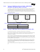
Table 9. Layout Recommendations for Topology 2B
L1 L2 Transmission Line Type
0.5” – 12.0” 0.5” – 6.5” Micro-strip
0.5” – 12.0” 0.5” – 6.5” Strip-line