
Guide

Mobile Intel Pentium 4 Processor–M and Mobile Intel Celeron Processor FSB Design Guidelines
R
32 Intel
®
852GM Chipset Platform Design Guide
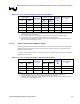
Parameter Processor Routing Guidelines
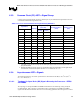
ADSTBn/p[1:0]# • An address strobe and its complement should be routed within ± 0.200 of the same Pad-to-
Pad length.
• The pad is defined as the attach point of the silicon die to the package substrate.
• Length must be added to the system board to compensate for package length differences.
• A layer transition may occur if the reference plane remains the same (Vss) and the layers are
of the same configuration (all stripline or all microstrip).
Common Clock
line lengths
0.5 inches – 6.5 inches
Topology Stripline
Routing priorities • All associated signals and strobes should be routed on same layer for entire length of bus.
• All signals should be referenced to Vss. Ideally, layer changes should not occur for any
signals.
• If a layer change must occur, reference plane must be Vss and the layers must all be of the
same configuration (all stripline or all microstrip for example).
Clock keepout
zones
A spacing requirement of 16-20 mils should be maintained around all clocks.
Trace Impedance 55 ohms ± 15%
Source
Synchronous
routing restrictions
• There are no length-matching routing restrictions between (or within) either the source-
synchronous data or address groups.
• As long as the strobe and associated line length routing guidelines are met for each group,
there is no need to length-match between the groups. For example, one data group may be
routed to the minimum allowable length while another data group could be routed to the
maximum allowable length.
• Simulations have verified that the FSB will still function correctly even under this extreme
condition.
Refer to the Intel
®
852GM Chipset GMCH Datasheet for GMCH package dimensions and refer to the
Mobile Intel
®
Pentium
®
4 Processor–M Datasheet for processor package dimensions.
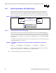
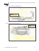
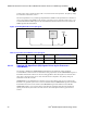
Figure 3. Cross-Sectional View of 2:1 Ratio
Reference Plane
2x
trace
trace
x
NOTE: This is the edge-to-edge trace spacing versus width.
A trace spacing to width ratio of 2 to 1 ensures a low crosstalk coefficient (based on geometries defined
in 8 layer reference stackup). All the effects of crosstalk are difficult to simulate. The timing and layout
guidelines for the processor have been created with the assumption of 2 to 1 trace spacing to width ratio.
A smaller ratio would have an unpredictable impact due to crosstalk.