
Guide

Platform Design Checklist
R
252 Intel
®
852GM Chipset Platform Design Guide
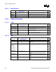
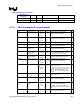
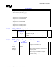
14.7.3. Hub Interface
Pin Name System
Pull-up/Pull-down
Notes
9
HLVREF
See Section
14.8.9.
Signal voltage level = 0.35 V ± 8%.
PSWING
See Section
14.8.9.
Signal voltage level = 2/3 of VCC1_2 or 0.8 V ± 8%.
HLZCOMP
27.4
Ω 1% pull-up to Vcc1_2
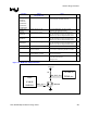
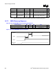
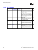
14.7.4. Graphics Interfaces
14.7.4.1. LVDS
Pin Name System
Pull-up/Pull-down
Notes
9
LIBG
1.5 k
Ω 1% pull-down to gnd
YAP[3:0]/YAM[3:0]
YBP[3:0]/YBM[3:0]
If any of these LVDS data pairs are unused, they can
be left as “no connect.”
CLKAP/CLKAM
CLKBP/CLKBM
If any of these LVDS clock pairs are not used, they can
be left as “no connect.”
LVREFH, LVREFL,
LVBG
These signals should be left as NC.
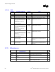
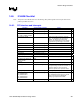
14.7.4.2. DVO
Pin Name System
Pull-up/Pull-down
Notes
9
DVORCOMP
40.2
Ω 1% pull-down to gnd
Trace should be 10-mil wide with 20-mil spacing.
GVREF
1 k
Ω 1% pull-up to Vcc1_5
1 k
Ω 1% pull-down to gnd
Signal voltage level = 1/2 of Vcc1_5. Need 0.1 µF
cap at pin.
DVOCD[11:0]
DVOCCLK
DVOCCLK#
DVOCHSYNC
DVOCVSYNC
DVOCBLANK#
If unused, these signals can be left as NC.
DVOCFLDSTL
100 k
Ω pull-down to gnd
Pull-down resistor required only if signal is unused
(10 k-100 k). It is up to DVO device to drive this
signal.
DVOBCINTR#
100 k
Ω pull-up to Vcc1_5
Pull-up resistor required only if signal is unused
(10 k-100 k). It is up to the DVO device to drive this
signal.
DVOBCCLKINT
100 k
Ω pull-down to gnd
Pull-down resistor required only if signal is unused
(10 k-100 k). It is up to the DVO device to drive this
signal.