
Data Sheet


Signal Description
108 Datasheet, Volume 1 of 2
6.2 PCI Express* Graphics (PEG) Signals
6.3 Direct Media Interface (DMI) Signals
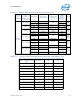
Table 6-4. System Memory Reference and Compensation Signals
Signal Name Description Dir.
Buffer
Type
Link
Type
Availability
DDR_RCOMP[2:0]
System Memory Resistance Compensation:
N/A A SE
All Processor Lines,
except S-Processor
Line
OPC_RCOMP
On-Package Cache resistance Compensation
from processor:
Note: Unconnected for Processors without OPC.
N/A A SE
Processors w/ On-
Package Cache
OPCE_RCOMP
Note: On-Package Cache resistance
Compensation from OPC: Unconnected
for Processors without OPC.
N/A A SE
Processors w/ On-
Package Cache
DDR_VTT_CNTL
System Memory Power Gate Control: When
signal is high – platform memory VTT regulator is
enable, output high.
When signal is low - Disables the platform memory
VTT regulator in C8 and deeper and S3.
O DDR4 SE All Processor Lines
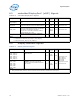
Table 6-5. PCI Express* Interface
Signal Name Description Dir.
Buffer
Type
Link
Type
Availability
PEG_RCOMP
Resistance Compensation for PCI Express
channels PEG and DMI.
N/A A SE
H and S-Processor
Line
PEG_RXP[15:0]
PEG_RXN[15:0]
PCI Express Receive Differential Pairs.
I
PCI
Express*
Diff
PEG_TXP[15:0]
PEG_TXN[15:0]
PCI Express Transmit Differential Pairs.
O
PCI
Express*
Diff
Table 6-6. DMI Interface Signals
Signal Name Description Dir.
Buffer
Type
Link
Type
Availability
DMI_RXP[3:0]
DMI_RXN[3:0]
DMI Input from PCH: Direct Media
Interface receive differential pairs.
I DMI Diff
H and S-Processor
Line
DMI_TXP[3:0]
DMI_TXN[3:0]
DMI Output to PCH: Direct Media Interface
transmit differential pairs.
O DMI Diff