
Data Sheet


Datasheet, Volume 1 of 2 107
Signal Description
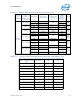
DDR0_CS#[3:0][1:0]
DDR1_CS#[3:0][1:0]
Chip Select: (1 per rank). These signals are used
to select particular SDRAM components during the
active state. There is one Chip Select for each
SDRAM rank.
O DDR4 SE
[1:0] applicable for All
Processor Lines.
[3:2] applicable only
in S and H-Processor
Line processors
DDR0_ODT[3:0][1:0]
DDR1_ODT[3:0][1:0]
On Die Termination: (1 per rank). Active SDRAM
Termination Control.
O DDR4 SE
[0,1] applicable for All
Processor Lines.
[3:2] applicable only
in S and H-Processor
Line processors
DDR0_MA[16:0]
DDR1_MA[16:0]
Address: These signals are used to provide the
multiplexed row and column address to the SDRAM.
• A[16:14] use also as command signals, Refer
ACT# signal description.
• A10 is sampled during Read/Write commands
to determine whether Autoprecharge should be
performed to the accessed bank after the
Read/Write operation.
HIGH: Autoprecharge;
LOW: no Autoprecharge).
• A10 is sampled during a Precharge command
to determine whether the Precharge applies to
one bank (A10 LOW) or all banks (A10 HIGH).
If only one bank is to be precharged, the bank
is selected by bank addresses.
• A12 is sampled during Read and Write
commands to determine if burst chop (on-the-
fly) will be performed.
HIGH, no burst chop;
LOW: burst chopped).
O DDR4 SE All Processor Lines
DDR0_ACT#
DDR1_ACT#
Activation Command: ACT# HIGH along with
CS# determines that the signals addresses below
have command functionality.
A16 use as RAS# signal
A15 use as CAS# signal
A14 use as WE# signal
O DDR4 SE All Processor Lines
DDR0_BG[1:0]
DDR1_BG[1:0]
Bank Group: BG[0:1] define to which bank group
an Active, Read, Write or Precharge command is
being applied.
BG0 also determines which mode register is to be
accessed during a MRS cycle.
O DDR4 SE
All processor lines
SO-DIMM, x8 DRAMs,
x16 DDP DRAMs
devices use BG[1:0].
x16 SDP DRAMs
devices use BG[0]
DDR0_BA[1:0]
DDR1_BA[1:0]
Bank Address: BA[1:0] define to which bank an
Active, Read, Write or Precharge command is being
applied. Bank address also determines which mode
register is to be accessed during a MRS cycle.
O DDR4 SE All Processor Lines
DDR0_ALERT#
DDR1_ALERT#
Alert: This signal is used at command training only.
It is getting the Command and Address Parity error
flag during training. CRC feature is not supported.
I DDR4 SE All Processor Lines
DDR0_PAR
DDR1_PAR
Command and Address Parity: These signals are
used for parity check.
O DDR4 SE All Processor Lines
DDR1_VREF_DQ Memory Reference Voltage for DQ: O A SE All -Processor Line
DDR_VREF_CA
Memory Reference Voltage for Command and
Address:
O A SE All Processor Lines
Table 6-3. DDR4 Memory Interface (Sheet 2 of 2)
Signal Name Description Dir.
Buffer
Type
Link
Type
Availability