
Data Sheet


Signal Description
106 Datasheet, Volume 1 of 2
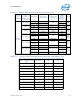
DDR0_CKE[3:0]
DDR1_CKE[3:0]
Clock Enable: (1 per rank) These signals are used
to:
• Initialize the SDRAMs during power-up.
• Power-down SDRAM ranks.
• Place all SDRAM ranks into and out of self-
refresh during STR.
O LPDDR3 SE
U and H -Processor
Line
DDR0_CS#[1:0]
DDR1_CS#[1:0]
Chip Select: (1 per rank). These signals are used
to select particular SDRAM components during the
active state. There is one Chip Select for each
SDRAM rank.
O LPDDR3 SE
U and H -Processor
Line
DDR0_ODT[3:0]
DDR1_ODT[3:0]
On Die Termination: Active Termination Control.
O LPDDR3 SE
U and H -Processor
Line
DDR0_CAA[9:0]
DDR1_CAA[9:0]
Command Address: These signals are used to
provide the multiplexed command and address to
the SDRAM.
O LPDDR3 SE
U and H -Processor
Line
DDR0_CAB[9:0]
DDR1_CAB[9:0]
Command Address: These signals are used to
provide the multiplexed command and address to
the SDRAM.
O LPDDR3 SE
U and H -Processor
Line
DDR0_VREF_DQ[1:0]
DDR1_VREF_DQ
Memory Reference Voltage for DQ:
O A SE U -Processor Line
DDR0_VREF_DQ
DDR1_VREF_DQ
Memory Reference Voltage for DQ:
O A SE H -Processor Line
DDR_VREF_CA
Memory Reference Voltage for Command and
Address:
OASE
U and H -Processor
Line
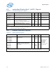
Table 6-3. DDR4 Memory Interface (Sheet 1 of 2)
Signal Name Description Dir.
Buffer
Type
Link
Type
Availability
DDR0_ECC[7:0]
DDR1_ECC[7:0]
ECC Data Buses: Data buses for ECC Check Byte.
I/O DDR4 SE
ECC UDIMM/SODIM
Modules with S and H-
Processor Line
processors
DDR0_DQ[63:0]
DDR1_DQ[63:0]
Data Buses: Data signals interface to the SDRAM
data buses.
I/O DDR4 SE All Processor Lines
DDR0_DQSP[87:0]
DDR0_DQSN[87:0]
DDR1_DQSP[87:0]
DDR1_DQSN[87:0]
Data Strobes: Differential data strobe pairs. The
data is captured at the crossing point of DQS during
read and write transactions.
I/O DDR4 Diff
The 9’th signals[8] are
applicable for UDIMM/
SODIM module with
ECC. in S and H-
Processor Line
processors. All
Processor Lines
DDR0_CKN[3:0][1:0]
DDR0_CKP[3:0][1:0]
DDR1_CKN[3:0][1:0]
DDR1_CKP[3:0][1:0]
SDRAM Differential Clock: Differential clocks
signal pairs, pair per rank. The crossing of the
positive edge of DDR0_CKP/DDR1_CKP and the
negative edge of their complement DDR0_CKN /
DDR1_CKN are used to sample the command and
control signals on the SDRAM.
O DDR4 Diff
[1:0] applicable for All
Processor Lines.
[3:2] applicable only
in S and H-Processor
Line processors
DDR0_CKE[3:0][1:0]
DDR1_CKE[3:0][1:0]
Clock Enable: (1 per rank). These signals are used
to:
• Initialize the SDRAMs during power-up.
• Power-down SDRAM ranks.
• Place all SDRAM ranks into and out of self-
refresh during STR (Suspend to RAM).
O DDR4 SE
[1:0] applicable for All
Processor Lines.
[3:2] applicable only
in S and H-Processor
Line processors.
Table 6-2. LPDDR3 Memory Interface (Sheet 2 of 2)
Signal Name Description Dir.
Buffer
Type
Link
Type
Availability