
Data Sheet


Datasheet, Volume 1 of 2 105
Signal Description
6 Signal Description
This chapter describes the processor signals. They are arranged in functional groups
according to their associated interface or category. The notations in the following table
are used to describe the signal type.
The signal description also includes the type of buffer used for the particular signal
(Refer the following table).
6.1 System Memory Interface
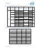
Table 6-1. Signal Tables Terminology
Notation Signal Type
I Input pin
O Output pin
I/O Bi-directional Input/Output pin
SE Single Ended Link
Diff Differential Link
CMOS CMOS buffers. 1.05V- tolerant
OD Open Drain buffer
LPDDR3 LPDDR3 buffers: 1.2V- tolerant
DDR4 DDR4 buffers: 1.2V-tolerant
A
Analog reference or output. May be used as a threshold voltage or for buffer
compensation
GTL Gunning Transceiver Logic signaling technology
Ref Voltage reference signal
Availability Signal Availability condition - based on segment, SKU, platform type or any other factor
Asynchronous
1
Signal has no timing relationship with any reference clock.
Note:
1. Qualifier for a buffer type.
Table 6-2. LPDDR3 Memory Interface (Sheet 1 of 2)
Signal Name Description Dir.
Buffer
Type
Link
Type
Availability
DDR0_DQ[63:0]
DDR1_DQ[63:0]
Data Buses: Data signals interface to the SDRAM
data buses.
I/O LPDDR3 SE
U and H -Processor
Line
DDR0_DQSP[7:0]
DDR0_DQSN[7:0]
DDR1_DQSP[7:0]
DDR1_DQSN[7:0]
Data Strobes: Differential data strobe pairs. The
data is captured at the crossing point of DQS during
read and write transactions.
I/O LPDDR3 Diff
U and H -Processor
Line
DDR0_CKN[1:0]
DDR0_CKP[1:0]
DDR1_CKN[1:0]
DDR1_CKP[1:0]
SDRAM Differential Clock: Differential clocks
signal pairs, pair per rank. The crossing of the
positive edge of DDR0_CKP/DDR1_CKP and the
negative edge of their complement DDR0_CKN /
DDR1_CKN are used to sample the command and
control signals on the SDRAM.
O LPDDR3 Diff
U and H -Processor
Line