
Specification Sheet


Electrical Specifications
52 Datasheet, Volume 1 of 2
5.5.2.2 PECI DC Specifications
5.5.2.3 System Reference Clock (BCLK{0/1/2}) DC Specifications
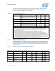
Symbol Definition and Conditions Min Max Units Figure Notes
1
V
In Input Voltage Range -0.15
0.15 + V
CCIO V1
V
Hysteresis Hysteresis 0.1*
V
CCIO —V
V
N
Negative-edge threshold voltage 0.275*
V
CCIO 0.500*
V
CCIO V Figure 5-1 2
V
P
Positive-edge threshold voltage 0.550*
V
CCIO 0.725*
V
CCIO V Figure 5-1 2
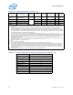
I
Source Pullup Resistance (V
OH
= 0.75*
V
CCIO
)
-6.00 — mA
I
Leak+ High impedance state leakage to
V
CCIO
(V
leak
=
V
OL
)
±50 ±200 μA
3, 4
R
ON High impedance leakage to GND (V
leak
= V
OH
)
41 11
C
Bus Bus capacitance per node — 10 pF 5
V
Noise Signal noise immunity above 300 MHz 0.100*
V
CCIO —
V
p-p
Output Edge Rate (50 ohm to V
SS
,
between
V
IL and V
IH
)
5 15 V/ns
Notes:
1. The input voltage range specifies an overshoot/undershoot that applies only to the PECI data signal and not to the V
TT
reference itself.
2. It is expected that the PECI driver will take into account, the variance in the receiver input thresholds and consequently, be
able to drive its output within safe limits (-0.150 V to 0.275*V
CCIO
for the low level and 0.725*V
CCIO
to V
CCIO
+0.150 V for
the high level).
3. V
CCIO nominal levels will vary between processor families. All PECI devices will operate at the VCCIO level determined by the
processor installed in the system.
4. The leakage specification applies to powered devices on the PECI bus.
5. Excessive capacitive loading on the PECI line may slow down the signal rise/fall times and consequently limit the maximum
bit rate at which the interface can operate.
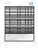
Symbol Parameter Signal Min Max Unit Figure Notes
1
V
BCLK_diff_ih Differential Input High
Voltage
Differential
0.150 N/A V
Figure 5-3 9
V
BCLK_diff_il Differential Input Low
Voltage
Differential
— -0.150 V
Figure 5-3 9
V
cross
(abs) Absolute Crossing Point Single Ended
0.250 0.550 V
Figure 5-4 and
Figure 5-5
2, 4, 7,
9
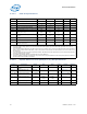
V
cross
(rel) Relative Crossing Point Single Ended 0.250 +
0.5*(VHavg -
0.700)
0.550 +
0.5*(VHavg -
0.700)
V
Figure 5-4 3, 4, 5,
9
Δ
V
cross Range of Crossing Points Single Ended N/A 0.140 V Figure 5-6 6, 9
V
TH Threshold Voltage Single Ended Vcross - 0.1 Vcross + 0.1 V 9