
Specification Sheet


Electrical Specifications
50 Datasheet, Volume 1 of 2
5.5.2 Signal DC Specifications
For additional specifications, refer to Section 1.8, “Related Documents.”
5.5.2.1 DDR4 Signal DC Specifications
For the next table, use Signal Group Table 5-6, “Signal Groups” to identify which
signals belong to each group.
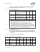
220 VID -0.198 VID -0.220 VID -0.242
230 VID - 0.208 VID - 0.230 VID - 0.252
Notes:
1. The V
CCIN_MIN
and V
CCIN_MAX
loadlines represent static and transient limits.
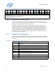
2. This table is intended to aid in reading discrete points on graph in Figure 5-2, “VCCIN Static and
Transient Tolerance Load Lines 1.0 mOHM” on page 50.
3. The loadlines specify voltage limits at the die measured at the V
CCIN_SENSE
and V
SS_VCCIN_SENSE
lands.
Voltage regulation feedback for voltage regulator circuits must also be taken from processor V
CCIN_SENSE
and V
SS_VCCIN_SENSE
lands.
4. The Adaptive Loadline Positioning slope is 1.00 m (mohm) with ±22mV TOB (Tolerance of Band).
Figure 5-2. VCCIN Static and Transient Tolerance Load Lines 1.0 mOHM
Table 5-13. V
CCIN
Static and Transient Tolerance for 1.0LL (Sheet 2 of 2)
I
CCIN
(A) V
CCIN_Max
(V) V
CCIN_Nom
(V) V
CCIN_Min
(V) Notes
Symbol Parameter Min Nom Max Units Notes
1
I
IL Input Leakage Current -1.4 — +1.4 mA 9
Data Signals
R
ON DDR4 Data Buffer On Resistance 25.5 30 34.5 ohm 6
Data ODT On-Die Termination for Data
Signals
42.5 50 57.5 ohm
8