
Specification Sheet


Datasheet, Volume 1 of 2 17
Interfaces
2 Interfaces
This chapter describes the functional behaviors supported by the processor. Topics
covered include:
• System Memory Interface
• PCI Express* Interface
• Direct Media Interface 3 (DMI3) / PCI Express* Interface
• Platform Environment Control Interface (PECI)
2.1 System Memory Interface
2.1.1 System Memory Technology Support
The Integrated Memory Controller (IMC) supports DDR4 protocols with four
independent 64-bit memory channels and supports one unbuffered DIMM per channel.
2.1.2 System Memory Timing Support
The IMC supports the following DDR4 Speed Bin, CAS Write Latency (CWL), and
command signal mode timings on the main memory interface:
•t
CL
= CAS Latency
•t
RCD
= Activate Command to READ or WRITE Command delay
•t
RP
= PRECHARGE Command Period
• CWL = CAS Write Latency
• Command Signal modes = 1n indicates a new command may be issued every clock
and 2n indicates a new command may be issued every two clocks. Command
launch mode programming depends on the transfer rate and memory
configuration.
2.2 PCI Express* Interface
This section describes the PCI Express* 3.0 interface capabilities of the processor. Refer
to the PCI Express* Base Specification for details of PCI Express*
3.0.
2.2.1 PCI Express* Architecture
Compatibility with the PCI addressing model is maintained to ensure that all existing
applications and drivers operate unchanged. The PCI Express* configuration uses
standard mechanisms as defined in the PCI Plug-and-Play specification.
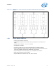
The PCI Express* architecture is specified in three layers – Transaction Layer, Data Link
Layer, and Physical Layer. The partitioning in the component is not necessarily along
these same boundaries. Refer to the following figure for the PCI Express* Layering
Diagram.