
User Manual

Electrical Specifications
56 Datasheet
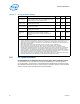
Notes:
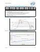
1. V
OS_MAX
is the measured overshoot voltage above V
CCIN_MAX
.
2. T
OS_MAX
is the measured time duration above V
CCIN_MAX
.
3. V
CCIN_MAX
= VID + TOB
5.6.2 Signal DC Specifications
For additional specifications, refer to the Related Documents Section.
5.6.2.1 DDR4 Signal DC Specifications
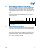
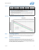
Table 5-13. V
CCIN
Overshoot Specifications
Symbol Parameter Min Max Units Figure Notes
V
OS_MAX
Magnitude of V
CCIN
overshoot above VID – 50 mV 5-5
T
OS_MAX
Time duration of V
CCIN
overshoot above
V
CCIN_Max
value at the new lighter load
–25 µs 5-5
Figure 5-5. V
CCIN
Overshoot Example Waveform
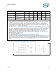
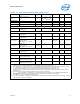
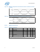
Table 5-14. DDR4 Signal DC Specifications (Sheet 1 of 2)
Symbol Parameter Min Nom Max Units Notes
1
I
IL
Input Leakage Current -1.4 – +1.4 mA 9
Data Signals
R
ON
DDR4 Data Buffer On Resistance 27 – 33 ohm 6
Data ODT
On-Die Termination for Data
Signals
45 – 55 ohm 8
Reference Clock and Command Signals
V
OL
Output Low Voltage
–
(V
CCD
/ 2)* (R
ON
/
(R
ON
+R
VTT_TERM
))
– V 2, 7