
User Manual

Datasheet 55
Electrical Specifications
5.6.1 Die Voltage Validation
Overshoot events that are < 10 ns in duration may be ignored. These measurements of
processor die level overshoot should be taken with a 100 MHz bandwidth limited
oscilloscope.
5.6.1.1 V
CCIN
Overshoot Specifications
The processor can tolerate short transient overshoot events where V
CCIN
exceeds the
VID voltage when transitioning from a high-to-low current load condition. This
overshoot cannot exceed VID + V
OS_MAX
(V
OS_MAX
is the maximum allowable overshoot
above VID). These specifications apply to the processor die voltage as measured across
the VCCIN_SENSE and VSS_VCCIN_SENSE lands.
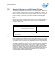
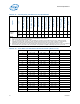
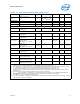
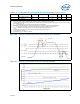
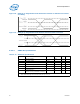
210 VID - 0.199 VID - 0.221 VID - 0.243
220 VID - 0.209 VID - 0.231 VID - 0.253
Notes:
1. The V
CCIN_MIN
and V
CCIN_MAX
loadlines represent static and transient limits. See Section 5.6.1, “Die
Voltage Validation” for V
CCIN
Overshoot specifications.
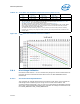
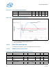
2. This table is intended to aid in reading discrete points on graph in Figure 5-4.
3. The loadlines specify voltage limits at the die measured at the VCCIN_SENSE and VSS_VCCIN_SENSE
lands. Voltage regulation feedback for voltage regulator circuits must also be taken from processor
VCCIN_SENSE and VSS_VCCIN_SENSE lands.
4. The Adaptive Loadline Positioning slope is 1.05 m (mohm) with ±22mV TOB (Tolerance of Band).
5. Processor core current (I
CCIN
) ranges are valid up to I
CCIN_MAX
of the processor SKU as defined in the
previous table.
Figure 5-4. V
CCIN
Static and Transient Tolerance Loadlines
Table 5-12. V
CCIN
Static and Transient Tolerance Processor (Sheet 2 of 2)
I
CCIN
(A) V
CCIN_Max
(V) V
CCIN_Nom
(V) V
CCIN_Min
(V) Notes