
User Manual

Datasheet 53
Electrical Specifications
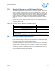
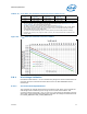
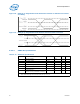
Table 5-10. Voltage Specification
Symbols Parameter
Voltage
Plane
Min Nom Max Unit Notes
1
V
CCIN
Input to Integrated
Voltage Regulator
V
CCIN
1.47 1.8 1.85 V
2, 3, 4, 5,
9, 12
V
VID_STEP
(V
CCIN
, V
CCD
)
VID step size during a
transition
– – 10.0 – mV 6
V
CCD (
V
CCD_01,
V
CCD_23)
I/O Voltage for DDR4
(Standard Voltage)
V
CCD
0.97*V
CCD_
NOM
1.2
1.044*V
C
CD_NOM
V
7, 8, 9,
10, 11
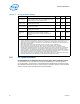
Notes:
1. Unless otherwise noted, all specifications in this table apply to all processors.
2. These voltages are targets only. A variable voltage source should exist on systems in the event that a different voltage is
required.
3. The V
CCIN
voltage specification requirements are measured across the remote sense pin pairs (V
CCIN_SENSE
and
V
SS_VCCIN_SENSE
) on the processor package. Voltage measurement should be taken with a DC to 100 MHz bandwidth
oscilloscope limit (or DC to 20MHz for older model oscilloscopes), using a 1.5 pF maximum probe capacitance, and 1 M
minimum impedance. The maximum length of the ground wire on the probe should be less than 5 mm to ensure external
noise from the system is not coupled in the scope probe.
4. Refer to Table 5-12, “V
CCIN
Static and Transient Tolerance Processor” on page 54 and corresponding Table 5-4, “V
CCIN
Static
and Transient Tolerance Loadlines” on page 55. The processor should not be subjected to any static V
CCIN
level that exceeds
the V
CCIN_MAX
associated with any particular current. Failure to adhere to this specification can shorten processor lifetime.
5. Minimum V
CCIN
and maximum I
CCIN
are specified at the maximum processor case temperature (T
CASE
) shown in the
Processor Thermal/Mechanical Specification and Design Guide (See Related Document Section). I
CCIN_MAX
is specified at
the relative V
CC_MAX
point on the V
CCIN
load line. The processor is capable of drawing I
CCIN_MAX
for up to 4 ms.
6. This specification represents the V
CCIN
reduction or V
CCIN
increase due to each VID transition. For Voltage Identification
(VID), see Table 5-3, “VR12.5 Reference Code Voltage Identification (VID) Table” on page 45.
7. Baseboard bandwidth is limited to 20 MHz.
8. DC + AC + Ripple = Total Tolerance
9. For SVID Power State Functions (SetPS) see Section 5.2.8.8, “SVID Power State Functions: SetPS” .
10. V
CCD
tolerance at processor pins. Required in order to meet ±5% tolerance at processor die.
11. The V
CCD01
, V
CCD23
voltage specification requirements are measured across vias on the platform. Choose V
CCD01
or V
CCD23
vias close to the socket and measure with a DC to 100MHz bandwidth oscilloscope limit (or DC to 20 MHz for older model
oscilloscopes), using 1.5 pF maximum probe capacitance, and 1M ohm minimum impedance. The maximum length of the
ground wire on the probe should be less than 5 mm to ensure external noise from the system is not coupled in the scope
probe.
12. V
CCIN
has a V
boot
setting of 0.0V and is not included in the PWRGOOD indication.
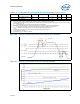
Figure 5-3. Serial VID Interface (SVID) Signals Clock Timings