
User Manual

Datasheet 47
Electrical Specifications
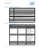
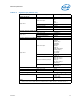
Table 5-4. Signal Description Buffer Types
Signal Description
Analog Analog reference or output. May be used as a threshold voltage or for buffer
compensation
Asynchronous
1
Signal has no timing relationship with any system reference clock.
CMOS CMOS buffers: 1.05V
DDR4 buffers: 1.2V
DMI2 Direct Media Interface Gen 2 signals. These signals are compatible with PCI Express* 2.0
and 1.0 Signaling Environment AC Specifications.
Intel
®
QPI Current-mode 9.6 GT/s, 8.0 GT/s, and 6.4 GT/s, forwarded-clock Intel QuickPath
Interconnect signaling
Open Drain CMOS Open Drain CMOS (ODCMOS) buffers: 1.05V tolerant
PCI Express* PCI Express* interface signals. These signals are compatible with PCI Express 3.0
Signalling Environment AC Specifications and are AC coupled. The buffers are not 3.3-V
tolerant. Refer to the PCIe specification.
Reference Voltage reference signal.
SSTL Source Series Terminated Logic (JEDEC SSTL_15)
Note:
1. Qualifier for a buffer type.
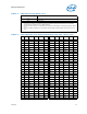
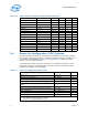
Table 5-5. Signal Groups (Sheet 1 of 3)
Differential/Single Ended Buffer Type Signal
DDR4 Reference Clocks
Differential SSTL Output DDR{0/1/2/3}_CLK_D[N/P][3:0]
DDR4 Command Signals
Single-ended SSTL Output
DDR{0/1/2/3}_ACT_N
DDR{0/1/2/3}_BA[1:0]
DDR{0/1/2/3}_BG[1:0]
DDR{0/1/2/3}_MA[17]
DDR{0/1/2/3}_MA[16]/_RAS_N
DDR{0/1/2/3}_MA[15]/_CAS_N
DDR{0/1/2/3}_MA[14]/_WE_N
DDR{0/1/2/3}_MA[13:0]
DDR{0/1/2/3}_PAR
DDR4 Control Signals
Single-ended SSTL Output
DDR{0/1/2/3}_CS_N[9:8]
DDR{0/1/2/3}CS_N[7]/CID[4]
DDR{0/1/2/3}CS_N[6]/CID[3]
DDR{0/1/2/3}_CS_N[5:4]
DDR{0/1/2/3}CS_N[3]/CID[1]
DDR{0/1/2/3}CS_N[2]/CID[0]
DDR{0/1/2/3}_CS_N[1:0]
DDR{0/1/2/3}_CID[2]
DDR{0/1/2/3}_ODT[5:0]
DDR{0/1/2/3}_CKE[5:0]
DDR4 Data Signals
Differential SSTL Input/Output DDR{0/1/2/3}_DQS_D[N/P][17:0]
Single ended SSTL Input/Output
DDR{0/1/2/3}_DQ[63:0]
DDR{0/1/2/3}_ECC[7:0]