
User Manual

Electrical Specifications
46 Datasheet
5.2.8.10 Reserved or Unused Signals
All Reserved (RSVD) signals must not be connected. Connection of these signals to
V
CCIN
, V
CCD
, V
SS
, or to any other signal (including each other) can result in component
malfunction or incompatibility with future processors.
For reliable operation, always connect unused inputs or bi-directional signals to an
appropriate signal level. Unused active high inputs should be connected through a
resistor to ground (V
SS
). Unused outputs maybe left unconnected; however, this may
interfere with some Test Access Port (TAP) functions, complicate debug probing, and
prevent boundary scan testing. A resistor must be used when tying bi-directional
signals to power or ground. When tying any signal to power or ground, a resistor will
also allow for system testability.
5.2.9 Reserved or Unused Signals
All Reserved (RSVD) signals must not be connected. Connection of these signals to
V
CCIN
, V
CCD
, V
SS
, or to any other signal (including each other) can result in component
malfunction or incompatibility with future processors.
For reliable operation, always connect unused inputs or bi-directional signals to an
appropriate signal level. Unused active high inputs should be connected through a
resistor to ground (V
SS
). Unused outputs maybe left unconnected; however, this may
interfere with some Test Access Port (TAP) functions, complicate debug probing, and
prevent boundary scan testing. A resistor must be used when tying bi-directional
signals to power or ground. When tying any signal to power or ground, a resistor will
also allow for system testability.
5.3 Signal Group Summary
Signals are grouped by buffer type and similar characteristics as listed in the following
table. The buffer type indicates which signaling technology and specifications apply to
the signals.
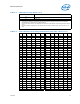
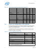
50 1.29 73 1.64 96 1.99 B9 2.34 DC 2.69 FF 3.04
51 1.30 74 1.65 97 2.00 BA 2.35 DD 2.70
52 1.31 75 1.66 98 2.01 BB 2.36 DE 2.71
53 1.320 76 1.67 99 2.02 BC 2.37 DF 2.72
54 1.33 77 1.68 9A 2.03 BD 2.38 E0 2.73
Notes:
1. 00h = Off State
2. VID Range HEX 01-32 are not used by the processor
3. For VID Ranges supported, see Table 5-10, “Voltage Specification” on page 53
4. V
CCD
is a fixed voltage of 1.20V
Table 5-3. VR12.5 Reference Code Voltage Identification (VID) Table (Sheet 2 of 2)
HEX VCCIN HEX VCCIN HEX VCCIN HEX VCCIN HEX VCCIN HEX VCCIN