
User Manual

Electrical Specifications
44 Datasheet
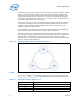
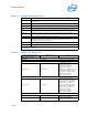
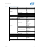
The VR may change its configuration to meet the processor's power needs with greater
efficiency. For example, it may reduce the number of active phases, transition from
CCM (Continuous Conduction Mode) to DCM (Discontinuous Conduction Mode) mode,
reduce the switching frequency or pulse skip, or change to asynchronous regulation.
For example, typical power states are 00h = run in normal mode; a command of 01h =
shed phases mode, and an 02h = pulse skip.
The VR may reduce the number of active phases from PS(00h)-to-PS(01h) or PS(00h)-
to-PS(02h) for example. There are multiple VR design schemes that can be used to
maintain a greater efficiency in these different power states. Work with your VR
controller suppliers for optimizations.
If a power state is not supported by the controller, the slave should acknowledge the
SetPS command and enter the lowest power state that is supported.
If the VR is in a low power state and receives a SetVID command moving the VID up,
then the VR exits the low power state to normal mode (PS0) to move the voltage up as
fast as possible. The processor must re-issue the low-power state (PS1 or PS2)
command if it is in a low current condition at the new higher voltage. See the following
figure for VR power state transitions.
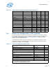
5.2.8.9 SVID Voltage Rail Addressing
The processor addresses three different voltage rail control segments within VR12.5
(V
CCIN
, V
CCD_01
, and V
CCD_23
). The SVID data packet contains a 4-bit addressing code.
Figure 5-2. Voltage Regulator (VR) Power State Transitions
Table 5-2. SVID Address Usage (Sheet 1 of 2)
PWM Address (HEX) Processor
00 V
CCIN
01 NA
02 V
CCD_01
03 +1 not used