
User Manual

Datasheet 41
Electrical Specifications
Clock multiplying within the processor is provided by the internal phase locked loop
(PLL), which requires a constant frequency BCLK{0/1}_DP, BCLK{0/1}_DN input, with
exceptions for spread spectrum clocking. DC specifications for the BCLK{0/1}_DP,
BCLK{0/1}_DN inputs are provided in Table 5-20, “Processor Asynchronous Sideband
DC Specifications” on page 62. These specifications must be met while also meeting
the associated signal quality specifications.
5.2.6 JTAG and Test Access Port (TAP) Signals
Due to the voltage levels supported by other components in the JTAG and Test Access
Port (TAP) logic, Intel recommends the processor be first in the TAP chain, followed by
any other components within the system. A translation buffer should be used to
connect to the rest of the chain unless one of the other components is capable of
accepting an input of the appropriate voltage. Two copies of each signal may be
required with each driving a different voltage level.
5.2.7 Processor Sideband Signals
The processor includes asynchronous sideband signals that provide asynchronous
input, output, or I/O signals between the processor and the platform or Platform
Controller Hub. Details can be found in Table 5-5, “Signal Groups” on page 47.
All processor Asynchronous Sideband input signals are required to be asserted/de-
asserted for a defined number of BCLKs in order for the processor to recognize the
proper signal state; these are outlined in Table 5-20, “Processor Asynchronous
Sideband DC Specifications” on page 62.
5.2.8 Power, Ground and Sense Signals
Processors also include various other signals including power/ground and sense points.
Details can be found in Table 5-5, “Signal Groups” on page 47.
5.2.8.1 Power and Ground Lands
All V
CCD
, V
CCIN
, and V
CCIO_IN
, and V
CCPECI
lands must be connected to their respective
processor power planes, while all V
SS
lands must be connected to the system ground
plane.
For clean on-chip power distribution, processors include lands for all required voltage
supplies. These are listed in the following table.
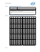
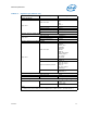
Table 5-1. Power and Ground Lands (Sheet 1 of 2)
Power and
Ground Lands
Number of
Lands
Comments
V
CCIN
173
Each V
CCIN
land must be supplied with the voltage determined by the
SVID Bus signals. Ta b l e 5 -3 defines the voltage level associated with
each core SVID pattern. Table 5-12 and Tab l e 5 - 4 represent V
CCIN
static
and transient limits.
V
CCD_01
V
CCD_23
56
Each V
CCD
land is connected to a switchable 1.20 V supply, provide
power to the processor DDR4 interface.
V
CCD
is also controlled by the SVID Bus. V
CCD
is the generic term for
V
CCD_01
and V
CCD_23
.