
User Manual

Signal Descriptions
38 Datasheet
4.10 Processor Power and Ground Supplies
§ §
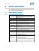
SOCKET_ID[1:0]
Socket ID Strap. Socket identification configuration straps for establishing
the PECI address, Intel
®
QPI Node ID, and other settings. This signal is used
in combination with FRMAGENT to determine whether the socket is a legacy
socket, bootable firmware agent is present, and DMI links are used in PCIe*
mode (instead of DMI2 mode). Each processor socket consumes one Node
ID, and there are 128 Home Agent tracker entries. This signal is pulled down
on the die. Refer to Table 5-6, “Signals with On-Die Weak Pull-Up/Pull-Down
Resistors” on page 50 for details.
TEST[3:0]
Test[3:0] must be individually connected to an appropriate power source or
ground through a resistor for proper processor operation.
TXT_AGENT
Intel
®
Trusted Execution Technology (Intel
®
TXT) Agent Strap.
0 = Default. The socket is not the Intel TXT Agent.
1 = The socket is the Intel TXT Agent.
The legacy socket (identified by SOCKET_ID[1:0] = 00b) with Intel TXT
Agent should always set the TXT_AGENT to 1b.
This signal is pulled down on the die. Refer to Table 5-6, “Signals with On-
Die Weak Pull-Up/Pull-Down Resistors” on page 50 for details.
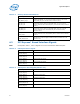
TXT_PLTEN
Intel Trusted Execution Technology (Intel TXT) Platform Enable Strap.
0 = The platform is not Intel TXT enabled. All sockets should be set to zero.
Scalable DP (sDP) platforms should choose this setting if the Node
Controller does not support Intel TXT.
1 = Default. The platform is Intel TXT enabled. All sockets should be set to
one. In a non-Scalable DP platform this is the default. When this is set,
Intel TXT functionality requires the user to explicitly enable Intel TXT
using BIOS setup.
This signal is pulled up on the die. Refer to Table 5-6, “Signals with On-Die
Weak Pull-Up/Pull-Down Resistors” on page 50 for details.
Table 4-15. Power and Ground Signals
Signal Name Description
V
CCIN
Input to the Integrated Voltage Regulator (IVR) for the processor cores,
lowest level caches (LLC), ring interface, PLL, IO, and home agent. It is
provided by a VR 12.5 compliant motherboard voltage regulator (MBVR) for
each CPU socket. The output voltage of this MBVR is controlled by the
processor, using the serial voltage ID (SVID) bus.
V
CCIN_SENSE
V
SS_VCCIN_SENSE
V
CCIN_SENSE
and V
SS_VCCIN_SENSE
are remote sense signals for V
CCIN
MBVR12.5 and are used by the voltage regulator to ensure accurate voltage
regulation. These signals must be connected to the voltage regulator
feedback circuit, which insures the output voltage remains within
specification.
V
CCD_01
V
CCD_23
Fixed 1.2V power supply for the processor system memory interface.
Provided by two MBVR 12.0 or 12.5 compliant regulators per CPU socket.
V
CCD_01
and V
CCD_23
are used for memory channels 0 &1 and 2 & 3,
respectively. The valid voltage of this supply (1.20V) is configured by BIOS
after determining the operating voltages of the installed memory. V
CCD_01
and V
CCD_23
will also be referred to as V
CCD
.
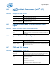
Note: The processor must be provided V
CCD_01
and V
CCD_23
for proper
operation, even in configurations where no memory is populated. A
MBVR 12.0 or 12.5 controller is required.
V
SS
Processor ground return.
V
CCIO_IN
IO voltage supply input.
V
CCPECI
Power supply for PECI. Refer to the PDG for specific connection options for
this pin.
Table 4-14. Miscellaneous Signals (Sheet 2 of 2)
Signal Name Description