
User Manual

Signal Descriptions
34 Datasheet
4.4 Intel
®
QuickPath Interconnect (Intel
®
QPI)
Signals
4.5 Platform Environment Control Interface (PECI)
Signal
4.6 System Reference Clock Signals
4.7 JTAG and TAP Signals
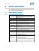
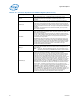
Table 4-8. Intel QPI Port 0 and 1 Signals
Signal Name Description
QPI{0/1}_CLKRX_DN/DP
Reference Clock Differential Input. These pins provide the PLL reference
clock differential input. 100 MHz typical.
QPI{0/1}_CLKTX_DN/DP
Reference Clock Differential Output. These pins provide the PLL reference
clock differential input. 100 MHz typical.
QPI{0/1}_DRX_DN/DP[19:0] QPI Receive data input.
QPI{0/1}_DTX_DN/DP[19:0] QPI Transmit data output.
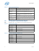
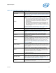
Table 4-9. Platform Environment Control Interface (PECI) Signal
Signal Name Description
PECI
PECI (Platform Environment Control Interface) is the serial sideband
interface to the processor and is used primarily for thermal, power and error
management.
Table 4-10. System Reference Clock (BCLK{0/1}) Signals
Signal Name Description
BCLK{0/1}_D[N/P]
Reference Clock Differential input.
These pins provide the required reference inputs to various PLLs inside the
processor, such as Intel QPI and PCIe. BCLK0 and BCLK1 run at 100 MHz
from the same clock source.
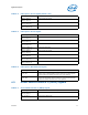
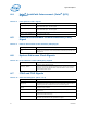
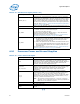
Table 4-11. JTAG and TAP Signals (Sheet 1 of 2)
Signal Name Description
BPM_N[7:0]
Breakpoint and Performance Monitor Signals: I/O signals from the processor
that indicate the status of breakpoints and programmable counters used for
monitoring processor performance. These are 100 MHz signals.
PRDY_N
Probe Mode Ready is a processor output used by debug tools to determine
processor debug readiness.
PREQ_N
Probe Mode Request is used by debug tools to request debug operation of
the processor.
TCK
TCK (Test Clock) provides the clock input for the processor Test Bus (also
known as the Test Access Port).
TDI
TDI (Test Data In) transfers serial test data into the processor. TDI provides
the serial input needed for JTAG specification support.