
User Manual

Signal Descriptions
32 Datasheet
4.2 PCI Express* Based Interface Signals
Note: PCI Express* Ports 1, 2 and 3 Signals are receive and transmit differential pairs.
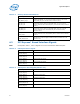
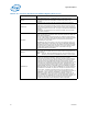
Table 4-2. Memory Channel Miscellaneous
Signal Name Description
DDR_RESET_C01_N
DDR_RESET_C23_N
System memory reset: Reset signal from processor to DRAM devices on the
DIMMs. DDR_RESET_C01_N is used for memory channels 0 and 1 while
DDR_RESET_C23_N is used for memory channels 2 and 3.
DDR_SCL_C01
DDR_SCL_C23
SMBus clock for the dedicated interface to the serial presence detect (SPD)
and thermal sensors (TSoD) on the DIMMs. DDR_SCL_C01 is used for
memory channels 0 and 1 while DDR_SCL_C23 is used for memory channels
2 and 3.
DDR_SDA_C01
DDR_SDA_C23
SMBus data for the dedicated interface to the serial presence detect (SPD)
and thermal sensors (TSoD) on the DIMMs. DDR_SDA_C01 is used for
memory channels 0 and 1 while DDR_SDA_C23 is used for memory
channels 2 and 3.
DDR01_VREF
DDR23_VREF
Voltage reference for CMD/ADD to the DIMMs. DDR01_VREF is used for
memory channels 0 and 1 while DDR23_VREF is used for memory channels
2 and 3.
DRAM_PWR_OK_C01
DRAM_PWR_OK_C23
Power good for V
CCD
rail used by the DRAM. This is an input signal used to
indicate the V
CCD
power supply is stable for memory channels 0 & 1 and
channels 2 & 3.
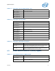
Table 4-3. PCI Express Port 1 Signals
Signal Name Description
PE1A_RX_DN[3:0]
PE1A_RX_DP[3:0]
PCIe Receive Data Input
PE1B_RX_DN[7:4]
PE1B_RX_DP[7:4]
PCIe Receive Data Input
PE1A_TX_DN[3:0]
PE1A_TX_DP[3:0]
PCIe Transmit Data Output
PE1B_TX_DN[7:4]
PE1B_TX_DP[7:4]
PCIe Transmit Data Output
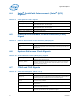
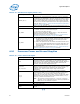
Table 4-4. PCI Express* Port 2 Signals (Sheet 1 of 2)
Signal Name Description
PE2A_RX_DN[3:0]
PE2A_RX_DP[3:0]
PCIe Receive Data Input
PE2B_RX_DN[7:4]
PE2B_RX_DP[7:4]
PCIe Receive Data Input
PE2C_RX_DN[11:8]
PE2C_RX_DP[11:8]
PCIe Receive Data Input
PE2D_RX_DN[15:12]
PE2D_RX_DP[15:12]
PCIe Receive Data Input
PE2A_TX_DN[3:0]
PE2A_TX_DP[3:0]
PCIe Transmit Data Output