
Specification Sheet


Intel
®
Xeon
®
Processor E5-1600/E5-2600/E5-4600 v2 Product Families 133
Datasheet Volume One of Two
Electrical Specifications
Clock multiplying within the processor is provided by the internal phase locked loop
(PLL), which requires a constant frequency BCLK{0/1}_DP, BCLK{0/1}_DN input, with
exceptions for spread spectrum clocking. DC specifications for the BCLK{0/1}_DP,
BCLK{0/1}_DN inputs are provided in Table 7 -1 7 . These specifications must be met
while also meeting the associated signal quality specifications outlined in Section 7.9.
7.1.6.1 PLL Power Supply
An on-die PLL filter solution is implemented on the processor. Refer to Tabl e 7 - 1 1 for
DC specifications.
7.1.7 JTAG and Test Access Port (TAP) Signals
Due to the voltage levels supported by other components in the JTAG and Test Access
Port (TAP) logic, Intel recommends the processor be first in the TAP chain, followed by
any other components within the system. Please refer to the
Intel® Xeon® Processor
E5-1600 v2/E5-2600 v2 Product Families – Boundary Scan Description Language
(BSDL) File for more details. A translation buffer should be used to connect to the rest
of the chain unless one of the other components is capable of accepting an input of the
voltage. Two copies of each signal may be required with each driving a different voltage
level.
7.1.8 Processor Sideband Signals
The processor include asynchronous sideband signals that provide asynchronous input,
output or I/O signals between the processor and the platform or Platform Controller
Hub. Details can be found in Table 7-5.
All Processor Asynchronous Sideband input signals are required to be
asserted/deasserted for a defined number of BCLKs in order for the processor to
recognize the proper signal state. Refer to Section 7.9 for applicable signal integrity
specifications.
7.1.9 Power, Ground and Sense Signals
Processors also include various other signals including power/ground and sense points.
Details can be found in Tab l e 7 -5 .
7.1.9.1 Power and Ground Lands
All V
CC
, V
CCPLL,
V
SA
, V
CCD,
V
TTA
, and V
TTD
lands must be connected to their respective
processor power planes, while all V
SS
lands must be connected to the system ground
plane. For clean on-chip power distribution, processors include lands for all required
voltage supplies. These are listed in Tab l e 7 -1 .
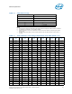
Table 7-1. Power and Ground Lands
Power and
Ground Lands
Number of
Lands
Comments
V
CC
208
Each V
CC
land must be supplied with the voltage determined by the
SVID Bus signals. Ta b le 7 -3 Defines the voltage level associated with
each core SVID pattern.Table 7-11, Figure 7-2, and Figure 7-4
represent V
CC
static and transient limits. VCC has a VBOOT setting of
0.0V.
V
CCPLL
3
Each V
CCPLL
land is connected to a 1.70 V supply, power the Phase
Lock Loop (PLL) clock generation circuitry. An on-die PLL filter
solution is implemented within the processor.