
Datasheet


Package Mechanical Specifications and Pin Information
52 Intel
®
Celeron
®
M Processor Datasheet
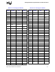
F26 VCCA[0] Power/Other
G1 RSVD Reserved
G2 VSS Power/Other
G3 VID[3] CMOS Output
G4 VID[4] CMOS Output
G5 VCC Power/Other
G6 VSS Power/Other
G21 VCC Power/Other
G22 VSS Power/Other
G23 VSS Power/Other
G24 D[22]# Source Synch
Input/
Output
G25 D[17]# Source Synch
Input/
Output
G26 VSS Power/Other
H1 RS[0]# Common Clock Input
H2 DRDY# Common Clock
Input/
Output
H3 VSS Power/Other
H4 VID[5] CMOS Output
H5 VSS Power/Other
H6 VCC Power/Other
H21 VSS Power/Other
H22 VCC Power/Other
H23 D[16]# Source Synch
Input/
Output
H24 D[20]# Source Synch
Input/
Output
H25 VSS Power/Other
H26 D[29]# Source Synch
Input/
Output
J1 VSS Power/Other
J2 LOCK# Common Clock
Input/
Output
J3 BPRI# Common Clock Input
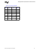
Table 24. Pin Listing by Pin Number
Pin
Number
Pin Name
Signal Buffer
Type
Direction
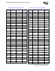
J4 VSS Power/Other
J5 VCC Power/Other
J6 VSS Power/Other
J21 VCC Power/Other
J22 VSS Power/Other
J23 D[23]# Source Synch
Input/
Output
J24 VSS Power/Other
J25 D[25]# Source Synch
Input/
Output
J26 DINV[1]# Source Synch
Input/
Output
K1 RS[1]# Common Clock Input
K2 VSS Power/Other
K3 HIT# Common Clock
Input/
Output
K4 HITM# Common Clock
Input/
Output
K5 VSS Power/Other
K6 VCCP Power/Other
K21 VSS Power/Other
K22 VCC Power/Other
K23 VSS Power/Other
K24 DSTBN[1]# Source Synch
Input/
Output
K25 D[31]# Source Synch
Input/
Output
K26 VSS Power/Other
L1 BNR# Common Clock
Input/
Output
L2 RS[2]# Common Clock Input
L3 VSS Power/Other
L4 DEFER# Common Clock Input
L5 VCCP Power/Other
L6 VSS Power/Other
L21 VCCP Power/Other
Table 24. Pin Listing by Pin Number
Pin
Number
Pin Name
Signal Buffer
Type
Direction