
Datasheet


Datasheet, Volume 1 87
Electrical Specifications
Notes:
1. V
AXG
is VID based rail.
2. The V
AXG_MIN
and V
AXG_MAX
loadlines represent static and transient limits.
3. The loadlines specify voltage limits at the die measured at the VAXG_SENSE and VSSAXG_SENSE lands.
Voltage regulation feedback for voltage regulator circuits must also be taken from processor VAXG_SENSE
and VSSAXG_SENSE lands.
4. PSx refers to the voltage regulator power state as set by the SVID protocol.
5. Each processor is programmed with a maximum valid voltage identification value (VID) that is set at
manufacturing and cannot be altered. Individual maximum VID values are calibrated during manufacturing
such that two processors at the same frequency may have different settings within the VID range. This
differs from the VID employed by the processor during a power management event (Adaptive Thermal
Monitor, Enhanced Intel SpeedStep Technology, or Low Power States).
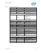
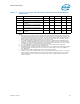
Table 7-6. Processor Graphics VID based (V
AXG
) Supply DC Voltage and Current
Specifications
Symbol Parameter Min Typ Max Unit Note
V
AXG
GFX_VID
Range
GFX_VID Range for V
AXG
0.2500 — 1.5200 V 1
LL
AXG
V
AXG
Loadline Slope 4.1 m 2, 3
V
AXG
TOB
V
CC
Tolerance Band
PS0, PS1
PS2
19
11.5
mV 2, 3, 4
V
AXG
Ripple
Ripple:
PS0
PS1
PS2
±10
±10
-10/+15
mV 2, 3, 4
I
AXG
Current for Processor Graphics
core
——35 A
I
AXG_TDC
Sustained current for Processor
Graphics core
——25 A
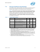
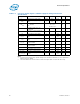
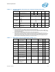
Table 7-7. DDR3 Signal Group DC Specifications (Sheet 1 of 2)
Symbol Parameter Min Typ Max Units Notes
1,7
V
IL
Input Low Voltage
——
SM_VREF
– 0.1
V2, 4, 9
V
IH
Input High Voltage SM_VREF
+ 0.1
——V3, 9
V
IL
Input Low Voltage
(SM_DRAMPWROK)
——
V
DDQ
*0.55
– 0.1
V8
V
IH
Input High Voltage
(SM_DRAMPWROK)
V
DDQ
*0.55
+ 0.1
——V8
V
OL
Output Low Voltage
—
(V
DDQ
/ 2)* (R
ON
/(R
ON
+R
TERM
))
—6
V
OH
Output High Voltage
—
V
DDQ
- ((V
DDQ
/ 2)*
(R
ON
/(R
ON
+R
TERM
))
—V4, 6
R
ON_UP(DQ)
DDR3 Data Buffer pull-
up Resistance
20 28.6 40 5
R
ON_DN(DQ)
DDR3 Data Buffer pull-
down Resistance
20 28.6 40 5
R
ODT(DQ)
DDR3 On-die
termination equivalent
resistance for data
signals
40 50 60
V
ODT(DC)
DDR3 On-die
termination DC working
point (driver set to
receive mode)
0.4*V
DDQ
0.5*V
DDQ
0.6*V
DDQ
V