
Datasheet


Electrical Specifications
Intel
®
Xeon
®
and Intel
®
Core™ Processors For Communications Infrastructure
Datasheet - Volume 1 of 2 May 2012
90 Document Number: 327405
-001
9.6 Reserved or Unused Signals
The following are the general types of reserved (RSVD) signals and connection
guidelines:
• RSVD_22, RSVD_33 and RSVD_44 - These pins must be shorted together and tied
to VCCP through 24.9 ohm 1% resistor.
• RSVD_[21:1], RSVD_[32:23], RSVD_[43:34] and RSVD_[57:45] - these signals
should not be connected.
Note: For more information regarding termination and layout guidelines, see the appropriate
platform design guide.
Arbitrary connection of these signals to V
CC
, V
CCIO
, V
DDQ
, V
CCPLL
, V
CCSA,
V
SS
, or to any
other signal (including each other) may result in component malfunction or
incompatibility with future processors. See Chapter 8.0, “Signal Description” for a pin
listing of the processor and the location of all reserved signals.
For reliable operation, always connect unused inputs or bi-directional signals to an
appropriate signal level. Unused active high inputs should be connected through a
resistor to ground (V
SS
). Unused outputs maybe left unconnected; however, this may
interfere with some Test Access Port (TAP) functions, complicate debug probing, and
prevent boundary scan testing. A resistor must be used when tying bi-directional
signals to power or ground. When tying any signal to power or ground, a resistor will
also allow for system testability. Resistor values should be within ±20% of the
impedance of the baseboard trace, unless otherwise noted in the appropriate platform
design guidelines. For details, see Table 8-12, “Processor Power Signals”.
9.7 Signal Groups
Signals are grouped by buffer type and similar characteristics as listed in Table 9-3. The
buffer type indicates which signaling technology and specifications apply to the signals.
All the differential signals, and selected DDR3 and Control Sideband signals have On-
Die Termination (ODT) resistors. Some signals do not have ODT and must be
terminated on the board.
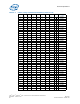
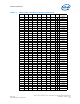
Table 9-3. Signal Groups (Sheet 1 of 3)
Signal Group
1
Type Signals
System Reference Clock
Differential CMOS Input BCLK, BCLK#
DDR3 Reference Clocks
2
Differential DDR3 Output
SA_CK[3:0], SA_CK#[3:0]
SB_CK[3:0], SB_CK#[3:0]
DDR3 Command Signals
2
Single Ended DDR3 Output
SA_RAS#, SB_RAS#, SA_CAS#,
SB_CAS#
SA_WE#, SB_WE#
SA_MA[15:0], SB_MA[15:0]
SA_BS[2:0], SB_BS[2:0]
SM_DRAMRST#
SA_CS#[3:0], SB_CS#[3:0]
SA_ODT[3:0], SB_ODT[3:0]
SA_CKE[3:0], SB_CKE[3:0]