
Datasheet


Signal Description
Intel
®
Xeon
®
and Intel
®
Core™ Processors For Communications Infrastructure
May 2012 Datasheet - Volume 1 of 2
Document Number: 327405
-001 75
8.4 PCI Express* Based Interface Signals
8.5 DMI
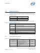
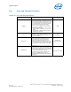
SM_DRAMRST#
DDR3 DRAM Reset: Reset signal from processor
to DRAM devices. One common to all channels.
0
CMOS
RSVD_[21:1],RSVD_[32:23],
RSVD_[43:34],RSVD_[57:45]
RESERVED: All signals in this group are RSVD pins
which must be left unconnected.
No Connect
RSVD_22, RSVD_33, RSVD_44
Terminated RESERVED: These pins must be
shorted together and tied to VCCP through 24.9 Ω
±1% resistor.
I
CMOS
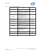
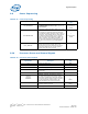
Table 8-6. PCI Express* Interface Signals
Signal Name Description
Direction/Buffer
Type
PCIE_ICOMPI
PCIE_ICOMPO
PCIE_RCOMPO
PCI Express* Compensation.
These pins must be shorted together and tied to VCCIO
through 24.9 Ω ±1% resistor.
I/Analog
PCIE1_RX[15:0]
PCIE1_RX#[15:0]
PCI Express* Receive Differential Pair. I/PCI Express*
PCIE1_TX[15:0]
PCIE1_TX#[15:0]
PCI Express* Transmit Differential Pair. O/PCI Express*
PCIE2_RX[3:0]
PCIE2_RX#[3:0]
PCI Express* Receive Differential Pair.
x4 Port
I/PCI Express*
PCIE2_TX[3:0]
PCIE2_TX#[3:0]
PCI Express* Transmit Differential Pair.
x4 Port
O/PCI Express*
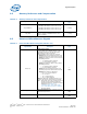
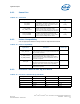
Table 8-7. DMI - Processor to PCH Serial Interface
Signal Name Description
Direction/Buffer
Type
DMI_RX[3:0]
DMI_RX#[3:0]
DMI Input from PCH: Direct Media Interface
receive differential pair.
I
DMI
DMI_TX[3:0]
DMI_TX#[3:0]
DMI Output to PCH: Direct Media Interface
transmit differential pair.
O
DMI
Table 8-5. Reset and Miscellaneous Signals (Sheet 2 of 2)
Signal Name Description
Direction/Buffer
Type