
Datasheet


Processor Configuration Registers
Intel
®
Xeon
®
and Intel
®
Core™ Processors For Communications Infrastructure
May 2012 Datasheet - Volume 1 of 2
Document Number: 327405
-001 161
Note: This document supplements or overrides the 2nd Generation Intel
®
Core™ Processor
Family Mobile Datasheet – Volume 1. For all information not contained in this
document, see the latest version of the 2nd Generation Intel
®
Core™ Processor Family
Mobile Datasheet – Volume 2.
11.11 Error Detection and Correction
If ECC is enabled and DIMMS with ECC are used, through an Error Correction Code
algorithm the memory controller is able to detect and correct single bit errors or detect
multiple bit errors. ECC increases the reliability of the DRAM devices by allowing single
bit errors to be fixed and detecting multi-bit errors but it requires additional bits to
store the error correction code. The ECC algorithm requires an 8-bit error correction
code. DIMMs with ECC are 72 bits wide, the first 64 bits are for data and the last 8 bits
are for the Check Bits.
Detection of correctable or uncorrectable errors are reported in the “ERRSTS - Error
Status” register. When either Single-bit correctable or Multi-bit uncorrectable errors are
detected, the column, row, bank, and rank that caused the error, and the error
syndrome, are logged in the ECC Error Log registers in the channel where the error
occurred. Channel 0 and Channel 1 errors are detailed in Section 11.5,
“ECCERRLOG0_C0 - ECC Error Log 0”, Section 11.6, “ECCERRLOG1_C0 - ECC Error Log
1”, Section 11.7, “ECCERRLOG0_C1 - ECC Error Log 0” and Section 11.8,
“ECCERRLOG1_C1 - ECC Error Log 1” respectively. If an uncorrectable error occurs
after a correctable error, then the address and syndrome information will be replaced
with the uncorrectable error information.
During the write cycle, ECC check bits are generated 1 per 8 bits of data by XORing a
particular combination of the written bits with an associated Check Bit. The result of
this function creates a syndrome byte that is visible via “Error Syndrome (ERRSYND):”,
(“ECCERRLOG0_C0 - ECC Error Log 0” or “ECCERRLOG0_C1 - ECC Error Log 0”).
Table 11-13 provides a lookup of the ERRSYND and defines the failing data bit.
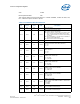
17 RW-L 0b Uncore
DIMM A number of ranks (DANOR):
0 = single rank
1 = dual rank
16 RW-L 0b Uncore
DIMM A select (DAS):
Selects which of the DIMMs is DIMM A - should
be the larger DIMM:
0 = DIMM 0
1 = DIMM 1
15:8 RW-L 00h Uncore
Size of DIMM B (DIMM_B_Size):
Size of DIMM B 256 MB multiples
7:0 RW-L 00h Uncore
Size of DIMM A (DIMM_A_Size):
Size of DIMM A 256 MB multiples
Table 11-12.Address Decode Channel 1 (Sheet 2 of 2)
Bit Access
Default
Value
RST/
PWR
Description
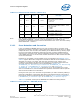
Table 11-13.Error Syndrome - ERRSYND (Sheet 1 of 3)
Syndrome
(ERRSYND)
Bit Locator
DQ/CB
Locator
0x00 No Error
0x01 64 CB0