
Datasheet


Processor Configuration Registers
Intel
®
Xeon
®
and Intel
®
Core™ Processors For Communications Infrastructure
Datasheet - Volume 1 of 2 May 2012
160 Document Number: 327405
-001
11.10 MAD_DIMM_CH1 - Address Decode Channel 1
B/D/F/Type: 0/0/0/MCHBAR_MCMAIN
Address Offset: 5008-500Bh
Default Value: 00600000h
Access: RW-L
Size: 32 bits
BIOS Optimal Default 00h
This register defines channel characteristics - number of DIMMs, number of ranks, size,
ECC, interleave options and ECC options.
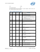
Table 11-12.Address Decode Channel 1 (Sheet 1 of 2)
Bit Access
Default
Value
RST/
PWR
Description
31:26 RO 0h Reserved (RSVD)
25:24 RW-L 00b Uncore
ECC is active in the channel (ECC):
00 =no ECC active in the channel
01 =ECC is active in IO, ECC logic is not active In
this case, on write accesses the data driven
on ECC byte is copied from DQ 7:0 (to be
used in training or IOSAV)
10 =ECC is disabled in IO, but ECC logic is
enabled (to be used in ECC4ANA mode)
11 =ECC active in both IO and ECC logic
23:23 RO 0h Reserved (RSVD)
22 RW-L 1b Uncore
Enhanced Interleave mode (Enh_Interleave):
0 = off
1 = on
21 RW-L 1b Uncore
Rank Interleave (RI):
0 = off
1 = on
20 RW-L 00b Uncore
DIMM B DDR width (DBW):
DBW: DIMM B width of DDR chips
0 = X8 chips
1 = X16 chips
19 RW-L 00b Uncore
DIMM A DDR width (DAW):
DAW: DIMM A width of DDR chips
0 = X8 chips
1 = X16 chips
18 RW-L 0b Uncore
DIMM B number of ranks (DBNOR):
0 = single rank
1 = dual rank