
Datasheet


Processor Configuration Registers
Intel
®
Xeon
®
and Intel
®
Core™ Processors For Communications Infrastructure
May 2012 Datasheet - Volume 1 of 2
Document Number: 327405
-001 155
11.4 SCICMD - SCI Command
B/D/F/Type: 0/0/0/PCI
Address Offset: CE-CFh
Default Value: 0000h
Access: RO; RW
Size: 16 bits
BIOS Optimal Default 0000h
This register enables various errors to generate an SCI DMI special cycle. When an
error flag is set in the ERRSTS register, it can generate an SERR, SMI, or SCI DMI
special cycle when enabled in the ERRCMD, SMICMD, or SCICMD registers respectively.
One and only one message type can be enabled.
11.5 ECCERRLOG0_C0 - ECC Error Log 0
B/D/F/Type: 0/0/0/MCHBAR MC0
Address Offset: 40C8-40CBh
Default Value: 00000000h
Access: ROS-V
Size: 32 bits
BIOS Optimal Default 0000h
This Channel 0 register is used to store the error status information in ECC enabled
configurations, along with the error syndrome and the rank and bank address
information of the address block of main memory of which an error (single bit or multi-
bit error) has occurred. The address fields represent the address of the first single or
the first multiple bit error occurrence after the error flag bits in the ERRSTS register
have been cleared by software. A multiple bit error will overwrite a single bit error.
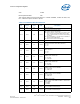
Table 11-6. SCI Command Registers
Bit Access
Default
Value
RST/
PWR
Description
15:2 RO 0h Reserved (RSVD)
1 RW 0b Uncore
SCI on Multiple-Bit DRAM ECC Error (DMESMI):
1 = The Host generates an SCI DMI message when it
detects a multiple-bit error reported by the DRAM
controller.
0 = Reporting of this condition via SCI messaging is
disabled. For systems not supporting ECC, this bit
must be disabled.
0 RW 0b Uncore
SCI on Single-bit ECC Error (DSESMI):
1 = The Host generates an SCI DMI special cycle
when the DRAM controller detects a single bit
error.
0 = Reporting of this condition via SCI messaging is
disabled. For systems that do not support ECC,
this bit must be disabled.