
Datasheet

Electrical Specifications
Intel
®
Xeon
®
and Intel
®
Core™ Processors For Communications Infrastructure
May 2012 Datasheet - Volume 1 of 2
Document Number: 327405
-001 105
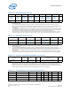
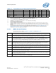
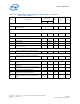
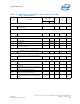
Table 9-19. DDR3 Electrical Characteristics and AC Timings at 1333 MT/s,
V
DDQ
= 1.5 V ±0.075 V
Symbol Parameter
Channel A
Channel B
Unit Figure Note
1,9
Max Min
System Memory Latency Timings
T
CL
– T
RCD
–
T
RP
CAS Latency – RAS to CAS Delay – Pre-charge
Command Period
9 – 9– 9 T
CK
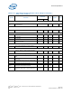
Electrical Characteristics
T
SLR_D
DQ[63:0], DQS[8:0], DQS#[8:0] Input Slew Rate 6.5 2.0 V/ns 2
System Memory Clock Timings
T
CK
CK Period 1.50 ns
T
CH
CK High Time 0.625 ns
T
CL
CK Low Time 0.625 ns
T
SKEW
Skew Between Any System Memory Differential
Clock Pair (CK/CKB)
100 ps
System Memory Command Signal Timings
T
CMD_CO
RAS#, CAS#, WE#, MA[14:0], BA[2:0] Edge
Placement Accuracy
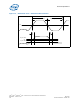
+145 -145 ps 9-5 3,4,6
System Memory Control Signal Timings
T
CTRL_CO
CS#[1:0], CKE[1:0], ODT[1:0] Edge Placement
Accuracy
+145 -145 ps 9-5 3,6
System Memory Data and Strobe Signal Timings
T
DVB
+T
DVA
DQ[63:0] Valid before DQS[8:0] Rising or Falling
Edge
500 ps 7
T
Su+HD
DQ Input Setup Plus Hold Time to DQS Rising or
Falling Edge
200 ps 9-6 1,2,7
T
DQS_CO
DQS Edge Placement Accuracy to CK Rising Edge
AFTER Write Levelling
+250 -250 ps 9-7 8
T
WPRE
DQS/DQS# Write Preamble Duration 1.0 T
CK
T
WPST
DQS/DQS# Write Postamble Duration 0.5 T
CK
T
DQSS
CK Rising Edge Output Access Time, Where a Write
Command Is Referenced, to the First DQS Rising
Edge
C
WL
x (T
CK
+ 4)
ns 5,6