
Datasheet

Electrical Specifications
Intel
®
Xeon
®
and Intel
®
Core™ Processors For Communications Infrastructure
May 2012 Datasheet - Volume 1 of 2
Document Number: 327405
-001 101
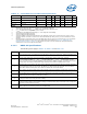
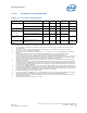
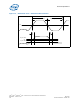
9.10.2.3 Input Device Hysteresis
The input buffers in both client and host models must use a Schmitt-triggered input
design for improved noise immunity. Use Figure 9-2 as a guide for input buffer design.
9.11 AC Specifications
The processor timings specified in this section are defined at the processor pads.
Therefore, proper simulation of the signals is the only means to verify proper timing
and signal quality.
See Chapter 10.0 for the processor pin listings and Chapter 8.0 for signal definitions.
Table 9-14 through Table 9-24 list the AC specifications associated with the processor.
The timings specified in this section should be used in conjunction with the processor
signal integrity models provided by Intel.
Note: Ensure to read all notes associated with a particular timing parameter.
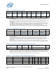
Ileak075 leakage current @ 0.75*V
CCIO
-0.13mA
Ileak100 leakage current @ V
CCIO
-0.10mA
Notes:
1. V
CCIO
supplies the PECI interface. PECI behavior does not affect V
TT
min/max specifications.
2. The leakage specification applies to powered devices on the PECI bus.
3. The PECI buffer internal pull up resistance measured at 0.75*V
CCIO
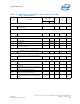
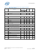
Table 9-13. PECI DC Electrical Limits (Sheet 2 of 2)
Symbol Definition and Conditions Min Max Units Notes
1
Figure 9-2. Input Device Hysteresis
Minimum V
P
Maximum V
P
Minimum V
N
Maximum V
N
PECI High Range
PECI Low Range
Valid Input
Signal Range
Minimum
Hysteresis
V
TTD
PECI Ground