
Datasheet


Electrical Specifications
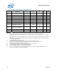
30 Datasheet
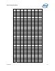
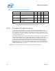
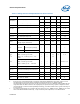
Table 9. AGTL+ Signal Group DC Specifications
Symbol Parameter Min Typ Max Unit Notes
1
V
CCP
I/O Voltage 1.00 1.05 1.10 V
GTLREF GTL Reference Voltage — 2/3 V
CCP
— V 6
R
COMP
Compensation Resistor 27.23 27.5 27.78 Ω 10
R
ODT
Termination Resistor — 55 — Ω 11
V
IH
Input High Voltage GTLREF+0.10 V
CCP
V
CCP
+0.10 V 3,6
V
IL
Input Low Voltage -0.10 0 GTLREF–0.10 V 2,4
V
OH
Output High Voltage V
CCP
–0.10 V
CCP
V
CCP
V 6
R
TT
Termination Resistance
46 [SS]
46 [CC]
55
61 [SS]
64 [CC]
Ω 7, 12
R
ON
(GTL
mode)
GTL Buffer on Resistance 21 25 29 Ω 5
I
LI
Input Leakage Current — — ±100 µA 8
Cpad Pad Capacitance 1.8 2.1 2.75 pF 9
NOTES:
1. Unless otherwise noted, all specifications in this table apply to all processor frequencies.
2. V
IL
is defined as the maximum voltage level at a receiving agent that will be interpreted as a logical low
value.
3. V
IH
is defined as the minimum voltage level at a receiving agent that will be interpreted as a logical high
value.
4. V
IH
and V
OH
may experience excursions above V
CCP
. However, input signal drivers must comply with the
signal quality specifications.
5. This is the pull-down driver resistance.
6. GTLREF should be generated from VCCP with a 1% tolerance resistor divider.
7. RTT is the on-die termination resistance measured at VOL of the AGTL+ output driver.
8. Specified with on-die RTT and RON are turned off.
9. Cpad includes die capacitance only. No package parasitics are included.
10. There are external resistor on the comp0 and comp2 pins.
11. On-die termination resistance, measured at 0.33*V
CCP
.
12. SS: source synchronous pins such as quad-pumped data bus and double-pumped address bus which
require a clock strobe. CC: Common clock pins.