
Desktop 4th Generation Specification Sheet


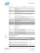
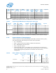
Table Of Contents
- Contents
- Revision History
- 1.0 Introduction
- 2.0 Interfaces
- 3.0 Technologies
- 3.1 Intel® Virtualization Technology (Intel® VT)
- 3.2 Intel® Trusted Execution Technology (Intel® TXT)
- 3.3 Intel® Hyper-Threading Technology (Intel® HT Technology)
- 3.4 Intel® Turbo Boost Technology 2.0
- 3.5 Intel® Advanced Vector Extensions 2.0 (Intel® AVX2)
- 3.6 Intel® Advanced Encryption Standard New Instructions (Intel® AES-NI)
- 3.7 Intel® Transactional Synchronization Extensions - New Instructions (Intel® TSX-NI)
- 3.8 Intel® 64 Architecture x2APIC
- 3.9 Power Aware Interrupt Routing (PAIR)
- 3.10 Execute Disable Bit
- 3.11 Supervisor Mode Execution Protection (SMEP)
- 4.0 Power Management
- 4.1 Advanced Configuration and Power Interface (ACPI) States Supported
- 4.2 Processor Core Power Management
- 4.3 Integrated Memory Controller (IMC) Power Management
- 4.4 PCI Express* Power Management
- 4.5 Direct Media Interface (DMI) Power Management
- 4.6 Graphics Power Management
- 5.0 Thermal Management
- 5.1 Desktop Processor Thermal Profiles
- 5.2 Thermal Metrology
- 5.3 Fan Speed Control Scheme with Digital Thermal Sensor (DTS) 1.1
- 5.4 Fan Speed Control Scheme with Digital Thermal Sensor (DTS) 2.0
- 5.5 Processor Temperature
- 5.6 Adaptive Thermal Monitor
- 5.7 THERMTRIP# Signal
- 5.8 Digital Thermal Sensor
- 5.9 Intel® Turbo Boost Technology Thermal Considerations
- 6.0 Signal Description
- 6.1 System Memory Interface Signals
- 6.2 Memory Reference and Compensation Signals
- 6.3 Reset and Miscellaneous Signals
- 6.4 PCI Express*-Based Interface Signals
- 6.5 Display Interface Signals
- 6.6 Direct Media Interface (DMI)
- 6.7 Phase Locked Loop (PLL) Signals
- 6.8 Testability Signals
- 6.9 Error and Thermal Protection Signals
- 6.10 Power Sequencing Signals
- 6.11 Processor Power Signals
- 6.12 Sense Signals
- 6.13 Ground and Non-Critical to Function (NCTF) Signals
- 6.14 Processor Internal Pull-Up / Pull-Down Terminations
- 7.0 Electrical Specifications
- 8.0 Package Mechanical Specifications
- 9.0 Processor Ball and Signal Information

Raw
Card
Version
DIMM
Capacity
DRAM
Device
Technology
DRAM
Organization
# of
DRAM
Devices
# of
Physical
Devices
Ranks
# of
Row / Col
Address
Bits
# of
Banks
Inside
DRAM
Page Size
B
2 GB 1 Gb 128 M X 8 16 2 14/10 8 8K
4 GB 2 Gb 256 M X 8 16 2 15/10 8 8K
4 GB 4 Gb 512 M X 8 8 1 15/10 8 8K
8 GB 4 Gb 512 M X 8 16 2 16/10 8 8K
Note: DIMM module support is based on availability and is subject to change.
Table 5. Supported SO-DIMM Module Configurations (AIO Only)
Raw Card
Version
DIMM
Capacity
DRAM
Organization
# of DRAM
Devices
# of Row/Col
Address Bits
# of Banks
Inside DRAM
Page Size
B
1 GB 128 M x 8 8 14/10 8 8K
2 GB 256 M x 8 8 15/10 8 8K
4 GB 512 M x 8 8 16/10 8 8K
F
2 GB 128 M x 8 16 14/10 8 8K
4 GB 256 M x 8 16 15/10 8 8K
8 GB 512 M x 8 16 16/10 8 8K
Note: System memory configurations are based on availability and are subject to change.
System Memory Timing Support
The IMC supports the following DDR3/DDR3L Speed Bin, CAS Write Latency (CWL),
and command signal mode timings on the main memory interface:
• tCL = CAS Latency
• tRCD = Activate Command to READ or WRITE Command delay
• tRP = PRECHARGE Command Period
• CWL = CAS Write Latency
• Command Signal modes = 1N indicates a new command may be issued every
clock and 2N indicates a new command may be issued every 2 clocks. Command
launch mode programming depends on the transfer rate and memory
configuration.
Table 6. DDR3 / DDR3L System Memory Timing Support
Segment Transfer Rate
(MT/s)
tCL (tCK) tRCD
(tCK)
tRP
(tCK)
CWL
(tCK)
DPC CMD
Mode
All segments
1333 8/9 8/9 8/9 7
1 1N/2N
2 2N
1600 10/11 10/11 10/11 8
1 1N/2N
2 2N
2.1.2
Processor—Interfaces
Desktop 4th Generation Intel
®
Core
™
Processor Family, Desktop Intel
®
Pentium
®
Processor Family, and Desktop Intel
®
Celeron
®
Processor Family
Datasheet – Volume 1 of 2 December 2013
20 Order No.: 328897-004