
Desktop 4th Generation Specification Sheet
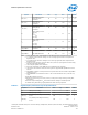

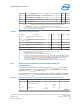


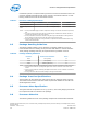


Table Of Contents
- Contents
- Revision History
- 1.0 Introduction
- 2.0 Interfaces
- 3.0 Technologies
- 3.1 Intel® Virtualization Technology (Intel® VT)
- 3.2 Intel® Trusted Execution Technology (Intel® TXT)
- 3.3 Intel® Hyper-Threading Technology (Intel® HT Technology)
- 3.4 Intel® Turbo Boost Technology 2.0
- 3.5 Intel® Advanced Vector Extensions 2.0 (Intel® AVX2)
- 3.6 Intel® Advanced Encryption Standard New Instructions (Intel® AES-NI)
- 3.7 Intel® Transactional Synchronization Extensions - New Instructions (Intel® TSX-NI)
- 3.8 Intel® 64 Architecture x2APIC
- 3.9 Power Aware Interrupt Routing (PAIR)
- 3.10 Execute Disable Bit
- 3.11 Supervisor Mode Execution Protection (SMEP)
- 4.0 Power Management
- 4.1 Advanced Configuration and Power Interface (ACPI) States Supported
- 4.2 Processor Core Power Management
- 4.3 Integrated Memory Controller (IMC) Power Management
- 4.4 PCI Express* Power Management
- 4.5 Direct Media Interface (DMI) Power Management
- 4.6 Graphics Power Management
- 5.0 Thermal Management
- 5.1 Desktop Processor Thermal Profiles
- 5.2 Thermal Metrology
- 5.3 Fan Speed Control Scheme with Digital Thermal Sensor (DTS) 1.1
- 5.4 Fan Speed Control Scheme with Digital Thermal Sensor (DTS) 2.0
- 5.5 Processor Temperature
- 5.6 Adaptive Thermal Monitor
- 5.7 THERMTRIP# Signal
- 5.8 Digital Thermal Sensor
- 5.9 Intel® Turbo Boost Technology Thermal Considerations
- 6.0 Signal Description
- 6.1 System Memory Interface Signals
- 6.2 Memory Reference and Compensation Signals
- 6.3 Reset and Miscellaneous Signals
- 6.4 PCI Express*-Based Interface Signals
- 6.5 Display Interface Signals
- 6.6 Direct Media Interface (DMI)
- 6.7 Phase Locked Loop (PLL) Signals
- 6.8 Testability Signals
- 6.9 Error and Thermal Protection Signals
- 6.10 Power Sequencing Signals
- 6.11 Processor Power Signals
- 6.12 Sense Signals
- 6.13 Ground and Non-Critical to Function (NCTF) Signals
- 6.14 Processor Internal Pull-Up / Pull-Down Terminations
- 7.0 Electrical Specifications
- 8.0 Package Mechanical Specifications
- 9.0 Processor Ball and Signal Information
Symbol Parameter Min Max Units Notes
1
V
IH
Input High Voltage (other GTL) V
CCIO_TERM
* 0.72 — V 2, 4
R
ON
Buffer on Resistance (CFG/BPM) 16 24 Ω —
R
ON
Buffer on Resistance (other GTL) 12 28 Ω —
I
LI
Input Leakage Current — ±150 μA 3
Notes: 1. Unless otherwise noted, all specifications in this table apply to all processor frequencies.
2. The V
CCIO_OUT
referred to in these specifications refers to instantaneous VCCIO_OUT.
3. For VIN between 0 V and V
CCIO_TERM
. Measured when the driver is tri-stated.
4. V
IH
and V
OH
may experience excursions above V
CCIO_TERM
. However, input signal drivers must
comply with the signal quality specifications.
Table 55. PCI Express* DC Specifications
Symbol Parameter Min Typ Max Units Notes
1
Z
TX-DIFF-DC
DC Differential Tx Impedance (Gen 1
Only)
80 — 120 Ω 1, 6
Z
TX-DIFF-DC
DC Differential Tx Impedance (Gen 2 and
Gen 3)
— — 120 Ω 1, 6
Z
RX-DC
DC Common Mode Rx Impedance 40 — 60 Ω 1, 4, 5
Z
RX-DIFF-DC
DC Differential Rx Impedance (Gen1
Only)
80 — 120 Ω 1
PEG_RCOMP Comp Resistance 24.75 25 25.25 Ω 2, 3
Notes: 1. See the PCI Express Base Specification for more details.
2. PEG_RCOMP should be connected to V
COMP_OUT
through a 25 Ω ±1% resistor.
3. Intel allows using 24.9 Ω ±1% resistors.
4. DC impedance limits are needed to ensure Receiver detect.
5. The Rx DC Common Mode Impedance must be present when the Receiver terminations are first
enabled to ensure that the Receiver Detect occurs properly. Compensation of this impedance can
start immediately and the 15 Rx Common Mode Impedance (constrained by RLRX-CM to 50 Ω
±20%) must be within the specified range by the time Detect is entered.
6. Low impedance defined during signaling. Parameter is captured for 5.0 GHz by RLTX-DIFF.
Platform Environment Control Interface (PECI) DC
Characteristics
The PECI interface operates at a nominal voltage set by V
CCIO_TERM
. The set of DC
electrical specifications shown in the following table is used with devices normally
operating from a V
CCIO_TERM
interface supply.
V
CCIO_TERM
nominal levels will vary between processor families. All PECI devices will
operate at the V
CCIO_TERM
level determined by the processor installed in the system.
Table 56. Platform Environment Control Interface (PECI) DC Electrical Limits
Symbol Definition and Conditions Min Max Units Notes
1
R
up
Internal pull up resistance 15 45 Ω 3
V
in
Input Voltage Range
-0.15
V
CCIO_TERM
+
0.15
V —
V
hysteresis
Hysteresis 0.1 *
V
CCIO_TERM
N/A V —
continued...
7.8.1
Electrical Specifications—Processor
Desktop 4th Generation Intel
®
Core
™
Processor Family, Desktop Intel
®
Pentium
®
Processor Family, and Desktop Intel
®
Celeron
®
Processor Family
December 2013 Datasheet – Volume 1 of 2
Order No.: 328897-004 103