8xC251TB, 8xC251TQ, Hardware Description Addendum to the 8xC251SA, 8xC251SB, 8xC251SP, 8xC251SQ, User’s Manual Release Date: December 2003 Order Number: 273138-002 The 8xC251Tx may contain design defects or errors known as errata which may cause the product to deviate from published specifications. Such errata are not covered by Intel's warranty. Current characterized errata are available on request.
Information in this document is provided in connection with Intel products. No license, express or implied, by estoppel or otherwise, to any intellectual property rights is granted by this document.
8xC251Tx Hardware Description REVISION HISTORY: Date Revision November 1997 001 Initial release of this document December 2003 002 Removed references to 8XC251TA, 8XC251TP 273138-002 Description December 2003 iii
8xC251Tx Hardware Description iv December 2003 273138-002
8xC251Tx Hardware Description 8xC251TB, 8xC251TQ Hardware Description Addendum to the 8xC251SA, 8xC251SB, 8xC251SP, 8xC251SQ, User’s Manual 1.0 INTRODUCTION TO THE 8xC251Tx 1.1 Comparing the 8xC251Tx and 8xC251Sx ..................................................................... 1 2.0 SIGNAL SUMMARY 3.0 THE SECOND SERIAL I/O PORT 3.1 Overview........................................................................................................................ 7 3.
8xC251Tx Hardware Description vi December 2003 273138-002
8xC251Tx Hardware Description 1.0 INTRODUCTION TO THE 8xC251Tx This Hardware Description describes the 8xC251TB, 8xC251TQ (referred to collectively as the 8xC251Tx) embedded microcontroller, which is the newest member of the MCS® 251 microcontroller family. The 8xC251Tx is pin and code compatible with the 8xC251Sx but is enhanced with the addition of new features. This document addresses the differences between the two members of the MCS 251 microcontroller family.
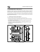
xC251Tx Hardware Description 2.0 SIGNAL SUMMARY Table 1. 8xC251Tx Signal Summary Address & Data Name Input/Output PLCC DIP AD0/P0.0 43 39 AD1/P0.1 42 38 AD2/P0.2 41 AD3/P0.3 40 AD4/P0.4 AD5/P0.5 PLCC DIP P1.0/T2 2 1 P1.1/T2EX 3 2 37 P1.2/EC/RXD1 4 3 36 P1.3/CEX0/TXD1 5 4 39 35 P1.4/CEX1 6 5 38 34 P1.5/CEX2 7 6 AD6/P0.6 37 33 P1.6/CEX3/WAIT# 8 7 AD7/P0.7 36 32 P1.7/CEX4/A17/WCLK 9 8 A8/P2.0 24 21 P3.0/RXD 11 10 A9/P2.1 25 22 P3.
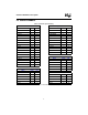
8xC251Tx Hardware Description Table 2. 8xC251Tx Signal Descriptions (Sheet 1 of 3) Signal Name Alternate Function Type Description A17 O Address Line 17. Output to memory as the 18th external address bit (A17) in extended bus applications, depending on the values of bits RD0 and RD1 in configuration byte UCONFIG0 (see Chapter 4, "Device Configuration," of the 8xC251SA, 8xC251SB, 8xC251SP, 8xC251SQ Embedded Microcontroller User’s Manual (272795). See also RD# and PSEN#. P1.
8xC251Tx Hardware Description Table 2. 8xC251Tx Signal Descriptions (Sheet 2 of 3) Signal Name Type Description Alternate Function P3.0 P3.1 P3.2 P3.3 P3.4 P3.5 P3.6 P3.7 I/O Port 3. This is an 8 bit, bidirectional I/O port with internal pullups PSEN# O Program Store Enable. Read signal output to external memory. Asserted for the address range specified by the configuration byte UCONFIG0, bits RD1:0. RD# O Read. Read signal output to external memory.
8xC251Tx Hardware Description Table 2. 8xC251Tx Signal Descriptions (Sheet 3 of 3) Signal Name Alternate Function Type Description VCC2 PWR Secondary Supply Voltage 2. This supply voltage connection is provided to reduce power supply noise. Connection of this spin to the +5V supply voltage is recommended. However, when using the ZX3 as a pin for pin replacement for the 8XC51FX, VCC2 can be unconnected without loss of compatibility (Not available on DIP). VSS GND Circuit Ground.
8xC251Tx Hardware Description Table 3.
8xC251Tx Hardware Description 3.0 THE SECOND SERIAL I/O PORT The second serial I/O port is functionally the same as the standard serial I/O port shared by both the 8xC251Tx and the 8xC251Sx. This section provides information about the new special function registers (SFRs) associated with the second serial port. Detailed operation and programming of the serial I/O ports can be obtained from Chapter 10 of the 8xC251SA, 8xC251SB, 8xC251SP, 8xC251SQ Embedded Microcontroller User’s Manual (272795).
8xC251Tx Hardware Description Table 5. Second Serial I/O Port Special Function Registers Mnemonic Description Address SBUF1 Serial Buffer 1. Two separate registers comprise the SBUF1 register. Writing to SBUF1 loads the transmit buffer; reading SBUF1 access the receive buffer 9BH SCON1 Serial Port Control 1. Selects the second serial I/O port operating mode.
8xC251Tx Hardware Description 3.2 Special Function Register Definitions The following describes the special function registers associated with the second serial I/O port and their bit definitions. 3.2.1 SCON1 Address: 9AH Reset Value: 0000 0000B Table 6. SCON1 Special Function Register Definitions Bit Number Bit Mnemonic Function 7 FE1SM0 Framing Error Bit 1: To Select this function, set the SMOD0 bit in the BGCON register. Set by hardware to indicate an invalid stop bit.
8xC251Tx Hardware Description 3.2.2 SBUF1 Address: 9BH Reset Value: xxxx xxxxB To send serial data, software writes a byte to SBUF1 and to receive serial data, software reads from SBUF1. 3.2.3 SADDR1 Address: AAH Reset Value: 0000 0000B Slave Individual Address Register1 (SADDR1) contains the device’s individual address for multiprocessor communications. 3.2.
8xC251Tx Hardware Description 3.2.6 IE1 Address: B1H Reset Value: xxxx xxx0B Table 8. IE1 Special Function Register Definitions Bit Mnemonic Bit Number Function 7-1 - Reserved 0 ES1 Second serial I/O port Interrupt Enable: Setting this bit enables the second serial I/O port interrupt 3.2.7 IPH1 Address: B3H Reset Value: xxxx xxx0B Table 9. IPH1 Special Function Register Definitions Bit Mnemonic Bit Number Function 7-1 - Reserved 0 IPH1.
8xC251Tx Hardware Description 4.0 EXTENDED DATA FLOAT TIMING The Extended Data Float Timing feature seeks to provide a solution to users that may be using slower memory devices. Essentially, this feature extends the TRHDZ1 AC timing specification to accommodate slower memory devices which require a longer period of dead time between a data and address bus cycles. This feature is controlled by a bit in the Configuration byte (UCONFIG1). Bit 3 of UCONFIG1 in the 8xC251Tx is defined as EDF#.
8xC251Tx Hardware Description Table 13 shows the effect of programming EDF# and WSB#[1:0] on the extended data float timing feature as well as the insertion of wait states for region 01:. It should be noted that enabling the extended data float timing allows region 01: to have 1 or 3 wait states inserted (depending on WSB#[1:0]) but not 0 or 2 wait states. Table 13.