
Microcontroller User's Manual


2-5
ARCHITECTURAL OVERVIEW
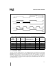
Figure 2-4. Effect of Clock Mode on Internal CLKOUT Frequency
2.4 EXTERNAL TIMING
You can control the output frequency on the CLKOUT pin by programming two uneraseable
PROM bits. Figure 2-5 illustrates the read-only USFR1, which reflects the state of the unerasable
PROM bits. You can select one of three frequencies: f/2, f/4, or f/8. As Figure 2-2 on page 2-3
shows, the configurable divider accepts the output of the clock generators (f/2) and further di-
vides that frequency to produce the desired output frequency. The CLK1:0 bits control the divisor
(divide f/2 by either 1, 2, or 4).
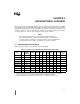
Table 2-3. Relationships Between Input Frequency, Clock Multiplier, and State Times
F
XTAL1
(Frequency
on XTAL1)
PLLEN Multiplier
f
(Input Frequency to
the Divide-by-two Circuit)
t
(Clock
Period)
State Time
4 MHz 0 1 4 MHz 250 ns 500 ns
8 MHz 0 1 8 MHz 125 ns 250 ns
12 MHz 0 1 12 MHz 83.5 ns 167 ns
16 MHz 0 1 16 MHz 62.5 ns 125 ns
20 MHz 0 1 20 MHz 50 ns 100 ns
4 MHz 1 2 8 MHz 125 ns 250 ns
8 MHz 1 2 16 MHz 62.5 ns 125 ns
10 MHz 1 2 20 MHz 50 ns 100 ns
Internal
CLKOUT
Internal
CLKOUT
t = 62.5ns
t = 31.25ns
T
XHCH
XTAL1
(16 MHz)
f
PLLEN = 1
f
PLLEN = 0
A3376-01