User Guide XB1 COM Express™ Module Document No.
User Guide XB1 COM Express Module Contents About this Manual . . . . . . . . . . . . . . . . . . . . . . . . . . . . . . . . . . . . . . . . . . . . . . . . . . . . . . . . . . . Edition History . . . . . . . . . . . . . . . . . . . . . . . . . . . . . . . . . . . . . . . . . . . . . . . . . . . . . . . . . Related Documents . . . . . . . . . . . . . . . . . . . . . . . . . . . . . . . . . . . . . . . . . . . . . . . . . . . . . Nomenclature . . . . . . . . . . . . . . . . . . . . . . . . . . . . . . . . .
User Guide XB1 COM Express Module Connectors . . . . . . . . . . . . . . . . . . . . . . . . . . . . . . . . . . . . . . . . . . . . . . . . . . . . . . . . . . PLD Programming Header ISPCON . . . . . . . . . . . . . . . . . . . . . . . . . . . . . . . . . . . J-COM . . . . . . . . . . . . . . . . . . . . . . . . . . . . . . . . . . . . . . . . . . . . . . . . . . . . . . . . Processor Debug Header PITP . . . . . . . . . . . . . . . . . . . . . . . . . . . . . . . . . . . . . . . P-SIO . . . . . . . . . . .
User Guide XB1 COM Express Module About this Manual This manual describes the technical aspects of the XB1 COM Express Module, required for installation and system integration. It is intended for the experienced user only. Edition History Ed. ©EKF Contents/Changes Author Date 1 User Manual XB1 COM Express Module, English, initial edition (Text #4162, File: xb1_uge.
User Guide XB1 COM Express Module Related Documents For ordering information refer to document XB1 COM Express Module Product Information, available at http://www.ekf.com/x/xb1/xb1_pie.pdf. Nomenclature Signal names used herein with an attached '#' designate active low lines. Trade Marks Some terms used herein are property of their respective owners, e.g.
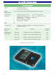
User Guide XB1 COM Express Module XB1 COM Express Module Features Feature Summary Feature Summary XB1 Form Factor PICMG COM Express R1.0 (COM.0), Basic Module form factor (125x95mm2), Pin-out Type 2 Processor Designed for Intel® Pentium® M Micro FC-BGA 479 processors (90nm Dothan), maximum junction temperature 100°C < XB1-060: 600MHz ULV Celeron® M (Banias 130nm), 400MHz FSB, 512KB L2 cache, 7W < < < XB1-100: 1.0GHz ULV Celeron® M (Dothan 373), 400MHz FSB, 512KB L2 cache, 5W XB1-140: 1.
User Guide XB1 COM Express Module Feature Summary XB1 Drivers < < Power Requirements +12V ±0.5V, tbd A max. @2.0GHz (tbd A WinXP idle mode) Environmental Conditions < < < < < < MTBF tbd EC Regulations • • Performance Rating Measured with PCMark2005 Intel graphics drivers Intel networking drivers Operating temperature: 0°C ... +70°C (CPU dependent) Storage temperature: -40°C ... +85°C, max. gradient 5°C/min Humidity 5% ... 95% RH non condensing Altitude -300m ... +3000m Shock 15g 0.
User Guide XB1 COM Express Module Short Description XB1 COM Express Module The XB1 is provided with a Gigabit Ethernet controller, and eight USB 2.0 ports for high speed communication. Four Serial ATA channels are available in addition to the legacy PATA I/F. The dual slot DIMM socket is suitable to address up to 2GB interleaved (symmetric) dual channel memory.
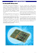
User Guide XB1 COM Express Module Benefits of the XB1 COM Express Module < < < < < < < < < < PICMG COM.0 Compliant Module Type 2 Pentium® M 2GHz (FSB 533MHz) PCI Express Chipset for Embedded Applications 2 x 1GB DDR2 Memory (Dual Channel Mode Capable) Dual-Screen Graphics Controller Video I/F SDVO, PEG, LVDS, VGA, TV Gigabit Ethernet Controller 4 x SATA I/F 8 x USB 2.0 Channels RoHS Compliant XB1 from Bottom ©EKF -9- ekf.
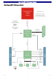
User Guide XB1 COM Express Module Block Diagram XB1 COM Express Module Pentium® M 760 • Pentium® M 745 1.8GHz • LV Pentium® M 738 1.4GHz • Celeron® M 370 1.5GHz • ULV Celeron® M 373 1.0GHz 2.
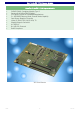
User Guide XB1 COM Express Module Assembly Drawing XB1 COM Express Module Top © EKF ekf.com CPU DDR2 SODIMM XB1 DDR2 SODIMM isp GAL GMCH J-RTC J-GP BAT + © EKF • XB1 COM Express Module • ekf.com A1 B1 J-COM A-B COM Express Module Connector C1 D1 J-COM C-D XB1 Bottom © EKF 1 ICH NIC ekf.com P-SIO SIO FWH 1 1 ©EKF ISPCON GP LED PG -11- P-ITP ekf.
User Guide XB1 COM Express Module Strapping Headers J-GP Jumper to reset BIOS CMOS RAM values J-RTC Jumper to reset RTC core of ICH6, not stuffed Connectors & Sockets ISPCON PLD programming connector, not stuffed J-COM A-B COM Express connector rows A and B (VGA, LVDS, TV, PCIe, SATA, Ethernet, USB, AC'97, SMB, LPC) J-COM C-D COM Express connector rows C and D (Dual SDVO / PEG, IDE, PCI) P-ITP CPU debug port P-SIO I/O connector for debugging (not stuffed), comprises PS/2 mouse/keyboard signals,
User Guide XB1 COM Express Module Microprocessor The XB1 COM Express Module is designed for use with Pentium® M and Celeron® M processors manufactured in 90nm technology (Dothan). These include also the Ultra Low-Voltage (ULV) Celeron® M and the Low-Voltage (LV) Pentium® M processors as listed below. The processors are housed in a Micro FC-BGA package for direct soldering to the PCB, i.e. the CPU chip cannot be removed or changed by the user.
User Guide XB1 COM Express Module Thermal Considerations In order to avoid malfunctioning of the XB1 COM Express Module, take care of appropriate cooling of the processor and system, e.g. by a cooling fan suitable to the maximum power consumption of the CPU chip actually in use. Please note, that the processors temperature is steadily measured by a special controller (LM87), attached to the onboard SMBus® (System Management Bus).
User Guide XB1 COM Express Module Main Memory The XB1 COM Express Module is equipped with two sockets for installing 200-pin SO-DIMM modules (module height = 1.25 inch). Supported are unbuffered DDR2 SO-DIMMs (VCC=1.8V) without ECC featuring on-die termination (ODT), according the PC2-3200 or PC2-4200 specification. Minimum memory size is 128MB; maximum memory size is 2GB.
User Guide XB1 COM Express Module Serial ATA Interface (SATA) The XB1 COM Express Module provides four serial ATA (SATA) ports, each capable of transferring 150MB/s. Integrated within the ICH6, the SATA controller features different modes to support also legacy operating systems. The SATA channels are available to the carrier board across the J-COM A-B connector. Available for download from Intel are drivers for popular operating systems, e.g. Windows® 2000, Windows® XP and Linux.
User Guide XB1 COM Express Module Graphics Subsystem The graphics subsystem is part of the versatile Intel i915GM Graphics/Memory Controller Hub (GMCH), and is also known as Intel Graphics Media Accelerator (GMA) 900. As an alternative, PCI Express based graphics is supported (requires discrete PEG controller present on the carrier board).
User Guide XB1 COM Express Module Real-Time Clock The XB1 COM Express Module has a time-of-day clock and 100-year calendar, integrated into the ICH6. A battery on the board keeps the clock current when the computer is turned off. The XB1 uses a Vanadium-Pentoxide-Lithium rechargeable battery, giving an autonomy of more than 50 days when fully loaded after 24 hours. The cell is free of memory effects and withstands deep discharging.
User Guide XB1 COM Express Module Watchdog/Reset The XB1 COM Express Module is provided with two supervisor circuits to monitor the supply voltages 1.8V, 3.3V, 5V, and to generate a clean power-on reset signal. The healthy state of the XB1 COM Express Module immideately after a reset is signalled by the LED PG (Power Good), indicating that all power voltages are within their specifications and the reset signal has been deasserted.
User Guide XB1 COM Express Module Installing and Replacing Components Before You Begin Warnings The procedures in this chapter assume familiarity with the general terminology associated with industrial electronics and with safety practices and regulatory compliance required for using and modifying electronic equipment. Disconnect the system from its power source and from any telecommunication links, networks or modems before performing any of the procedures described in this chapter.
User Guide XB1 COM Express Module Installing the Board Warning This procedure should be done only by qualified technical personnel. Disconnect the system from its power source before doing the procedures described here. Failure to disconnect power, or telecommunication links before you open the system or perform any procedures can result in personal injury or equipment damage.
User Guide XB1 COM Express Module Removing the Board Warning This procedure should be done only by qualified technical personnel. Disconnect the system from its power source before doing the procedures described here. Failure to disconnect power, or telecommunication links before you open the system or perform any procedures can result in personal injury or equipment damage.
User Guide XB1 COM Express Module EMC Recommendations In order to comply with the CE regulations for EMC, it is mandatory to observe the following rules: C The chassis or rack including other boards in use must comply entirely with CE C Close all board slots not in use with a blind front panel C Front panels must be fastened by built-in screws C Cover any unused front panel mounted connector with a shielding cap C External communications cable assemblies must be shielded (shield connected only at o
User Guide XB1 COM Express Module Installing or Replacing the Memory Modules Note: If you decide to replace the memory, observe the precautions in 'Before You Begin' By default, the XB1 COM Express Module comes fully equipped and tested with two DDR2 SDRAM memory modules. So normally there should be no need to install the memory modules. The XB1 COM Express Module requires at least one PC2-3200/4200 (400/533MHz) DDR2 SDRAM SODIMM module.
User Guide XB1 COM Express Module Technical Reference Local PCI Devices The following table shows the on-board PCI devices and their location within the PCI configuration space. These devices reside mainly within the i915GM chipset. 1) 2) ©EKF Bus Number Device Number Function Number Vendor ID Device ID Description 0 0 0 0x8086 0x2590 Host Bridge 0 2 0 0x8086 0x2592 Internal Graphics Device 0 2 1 0x8086 0x2792 Int. Graphics Config. Regs.
User Guide XB1 COM Express Module Local SMB Devices The XB1 COM Express Module contains a few devices that are attached to the System Management Bus (SMBus). These are the clock generation chip, the SPD EEPROMs on the SO-DIMM memory modules, a general purpose serial EEPROM and a supply voltage and CPU temperature controlling device in particular. Other devices could be connected to the SMB on the carrier board across J-COM A-B.
User Guide XB1 COM Express Module GPIO Usage GPIO Usage ICH6 XB1 COM Express Module GPIO Usage ICH6 GPIO Type Tol. Function GPI 0 I 5V EXCD1_CPPE# PCI ExpressCard PCI Express capable card 1 request GPI 1 I 5V EXCD0_CPPE# PCI ExpressCard PCI Express capable card 0 request GPI 2 I 5V PG_VR33 Power Good signal from 3.
User Guide XB1 COM Express Module XB1 COM Express Module GPIO Usage ICH6 GPIO Type Tol. Function Description GPI 30 I 3.3V BOARD_CFG2 Board configuration options line 2 GPI 31 I 3.3V BOARD_CFG3 Board configuration options line 3 GPIO 32 O 3.3V GPIO 33 O 3.3V NC1_OFF# Enable Ethernet Controller NC1 GPIO 34 I/O 3.3V ICH_GPIO34 for future use as PLD control signal (either input or output) GPI 40 I 5V PG_VR18 GPI 41 I 3.3V LPC_DRQCOM# GPO 48 O 3.3V GPO 49 OD 1.
User Guide XB1 COM Express Module GPIO Usage SIO XB1 COM Express Module GPIO Usage SIO 1) GPIO Type Tol.
User Guide XB1 COM Express Module Configuration Jumpers Reset Jumper BIOS CMOS RAM Values (J-GP) The jumper J-GP is used to reset the contents of the battery backed CMOS RAM to their default state. The BIOS uses the CMOS to store configuration values, e.g. the order of boot devices. Using this jumper is appropriate only, if it is not possible to enter the setup screen of the BIOS. To restore the CMOS RAM, install a short circuit jumper on JGP and perform a system reset.
User Guide XB1 COM Express Module Connectors Caution Some of the internal connectors provide operating voltage (3.3V and 5V) to devices inside the system chassis, such as internal peripherals. Not all of these connectors are overcurrent protected. Do not use these internal connectors for powering devices external to the computer chassis. A fault in the load presented by the external devices could cause damage to the board, the interconnecting cable and the external devices themselves.
User Guide XB1 COM Express Module J-COM J-COM is the pair of connectors which serves as interface between the XB1 COM Express Module and the carrier board. The assembly is composed of two double-row, high speed, 0.5mm pitch plugs. Each row has 110 leads, i.e. J-COM provides 440 contact positions in total. The COM.0 specification assigns each row a letter A, B and C, D. For Type 1 COM Express modules, rows A and B are sufficient (single connector, 220 leads).
User Guide XB1 COM Express Module ©EKF A B # C D GND GND 31 GND GND AC_BITCLK SPKR 32 PCI_AD14 PCI_PAR AC_SDOUT I2C_CK 33 PCI_CBE1# PCI_SERR# BIOS_DISABLE# I2C_DAT 34 PCI_PERR# PCI_STOP# THRMTRIP# THRM# 35 PCI_LOCK# PCI_TRDY# USB_6N USB_7N 36 PCI_DEVSEL# PCI_FRAME# USB_6P USB_7P 37 PCI_IRDY# PCI_AD16 USB_OC67# USB_OC45# 38 PCI_CBE2# PCI_AD18 USB_4N USB_5N 39 PCI_AD17 PCI_AD20 USB_4P USB_5P 40 PCI_AD19 PCI_AD22 GND GND 41 GND GND USB_2N USB_3N 4
User Guide XB1 COM Express Module A B # C D GND GND 60 GND GND PCIE_TX2+ PCIE_RX2+ 61 PEG_RX3+ SDVOB_CLK+ PEG_TX3+ PCIE_TX2- PCIE_RX2- 62 PEG_RX3- SDVOB_CLK- PEG_TX3- GPI1 GPO3 63 RSVD RSVD PCIE_TX1+ PCIE_RX1+ 64 RSVD RSVD PCIE_TX1- PCIE_RX1- 65 PEG_RX4+ SDVOC_RED+ PEG_TX4+ 66 PEG_RX4- SDVOC_RED- PEG_TX4- GND PE_WAKE# (WAKE0#) GPI2 WAKE1# 67 RSVD GND PCIE_TX0+ PCIE_RX0+ 68 SDVOC_INT+ PEG_RX5+ SDVOC_GRN+ PEG_TX5+ PCIE_TX0- PCIE_RX0- 69 SDVOC_INT- PEG_RX5-
User Guide XB1 COM Express Module A B # C D GND GND 90 GND GND RSVD VGA_GREEN 91 PEG_RX12+ PEG_TX12+ RSVD VGA_BLUE 92 PEG_RX12- PEG_TX12- GPO0 VGA_HSYNC 93 GND GND RSVD VGA_VSYNC 94 PEG_RX13+ PEG_TX13+ RSVD VGA_DDCCL (VGA_I2C_CK) 95 PEG_RX13- PEG_TX13- GND VGA_DDCDAT (VGA_I2C_DAT) 96 GND GND +12V TV_DAC_A 97 RSVD PEG_ENABLE# +12V TV_DAC_B 98 PEG_RX14+ PEG_TX14+ +12V TV_DAC_C 99 PEG_RX14- PEG_TX14- GND GND 100 GND GND +12V +12V 101 PEG_RX15+ PEG
User Guide XB1 COM Express Module Processor Debug Header PITP This FFC style connector (Molex 52435-2872) can be used to attach an emulator probe to the board. This is a valuable tool when debugging hardware or tracing software. The connector PITP is situated at the bottom side of the board.
User Guide XB1 COM Express Module P-SIO The connector P-SIO is normally not stuffed. The mature PS/2 and UART ports have been overcome by USB in most applications. For low level debugging however, these interfaces can be very useful (e.g. the BIOS can communicate across the serial I/O). Please contact EKF before ordering the XB1 COM Express Module, if the P_SIO connector is required by the user. P-SIO MS_CLK 1 2 MS_DAT KB_CLK 3 4 KB_DAT COM_CTS# (TTL) 5 6 COM_RTS# (TTL) 1.
User Guide XB1 COM Express Module 95.00 Board Dimensions 91.00 Top View (connectors seen through board) COM Express Basic Module © EKF ekf.com 4.00 6.00 18.00 D1 4.00 A1 16.50 74.20 80.00 121.00 125.00 ©EKF -38- ekf.
User Guide XB1 COM Express Module Top View, Bottom View XB1 Top View XB1 Bottom View ©EKF -39- ekf.
User Guide XB1 COM Express Module Literature Theme Document Title Origin COM Express PICMG® COM.0 COM Express™ Module Base Specification Revision 1.0 2005-07 www.picmg.org Ethernet IEEE Std 802.3, 2000 Edition standards.ieee.org PCI Express PCI Express Base Specification 1.1 www.pcisig.com Serial ATA Serial ATA Revision 2.5 www.serialata.org USB Universal Serial Bus Specification www.usb.org EKF Elektronik GmbH Philipp-Reis-Str. 4 59065 HAMM Germany Fax. +49 (0)2381/6890-90 Tel.