82540EP Gigabit Ethernet Controller Networking Silicon Datasheet Revision 1.
INFORMATION IN THIS DOCUMENT IS PROVIDED IN CONNECTION WITH INTEL PRODUCTS. NO LICENSE, EXPRESS OR IMPLIED, BY ESTOPPEL OR OTHERWISE, TO ANY INTELLECTUAL PROPERTY RIGHTS IS GRANTED BY THIS DOCUMENT.
Networking Silicon — 82540EP Revision History Datasheet Date Revision Notes Apr 2002 0.25 Nov 2002 1.0 Initial Release Changed document status to Intel Confidential. Jan 2003 1.1 Section 1.0. Replaced Block Diagram Section 2.6. Added Table footnote Section 4.1, 4.2, 4.3. Replaced tables Section 5.1. Added Visual Pin Reference Section 4.4 Removed Power Supply Characteristics; added note to I/O Characteristics Section 5.0 Replaced Pinout Diagram Apr 2003 1.2 Removed confidential status.
82540EP — Networking Silicon Note: iv This page is intentionally left blank.
Networking Silicon — 82540EP Contents 1.0 Introduction......................................................................................................................... 1 1.1 1.2 1.3 2.0 Features of the 82540EP Gigabit Ethernet Controller........................................................ 5 2.1 2.2 2.3 2.4 2.5 2.6 2.7 3.0 3.3 3.4 3.5 3.6 3.7 Signal Type Definitions.......................................................................................... 9 PCI Bus Interface .............
82540EP — Networking Silicon 4.5.3 5.0 Package and Pinout Information ...................................................................................... 27 5.1 5.2 5.3 5.4 5.5 vi EEPROM Interface................................................................................. 26 Device Identification ........................................................................................... 27 Package Information ......................................................................................
Networking Silicon — 82540EP 1.0 Introduction The Intel® 82540EP Gigabit Ethernet Controller is a single, compact component with an integrated Gigabit Ethernet Media Access Control (MAC) and physical layer (PHY) functions.
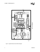
2540EP — Networking Silicon PCI i/f PCI I/F ACPI Target Control LED ASF PHY GMII MAC Core TX MAC TX Link RX Data Statistics Filter RX MAC CSR Register Access RX Data Mgmt FIFOs SMBus Interface Manageability MDIO Tx Arb 82540EP Architecture Flash Interface Flash TX Out Flow Ctrl RX In CSR Register Access Control, Status & Interrupt Registers Target Logic DMA TX descriptor TX engine FIFOs RX descriptor RX engine FIFOs 64K bytes Packet Buffer TX Data PCI Core Master write FIFO M
Networking Silicon — 82540EP 1.1 Document Scope This document contains datasheet specifications for the 82540EP Gigabit Ethernet Controller, including signal descriptions, DC and AC parameters, packaging data, and pinout information. 1.2 Reference Documents This application assumes that the designer is acquainted with high-speed design and board layout techniques.
82540EP — Networking Silicon Note: 4 This page is intentionally left blank.
Networking Silicon — 82540EP 2.0 Features of the 82540EP Gigabit Ethernet Controller 2.1 PCI Features Features Benefits • PCI Revision 2.3 support for 32-bit wide interface at 33 MHz and 66 MHz Algorithms that optimally use advanced PCI, MWI, MRM, and MRL commands • Application flexibility for LAN on Motherboard (LOM) or embedded solutions 64-bit addressing for systems with more than 4 Gigabytes of physical memory Support for new PCI 2.
82540EP — Networking Silicon 2.
Networking Silicon — 82540EP 2.5 Manageability Features Features Manageability features: SMB port, ASF 1.0, ACPI, Wake on LAN, and PXE On-board SMB port Compliance with PCI Power Management 1.1 and ACPI 2.0 register set compliant including: • D0 and D3 power states • Network Device Class Power Management Specification 1.1 • PCI Specification 2.2 SNMP and RMON statistic counters SDG 3.0, WfM 2.
82540EP — Networking Silicon 2.6 Additional Device Features Features Four activity and link indication outputs that directly drive LEDs Benefits • Link and activity indications (10, 100, and 1000 Mbps) on each port • Software definable function (speed, link, and activity) and blinking allowing flexible LED implementations Internal PLL for clock generation can use a 25 MHz crystal • Lower component count and system cost JTAG (IEEE 1149.
Networking Silicon — 82540EP 3.0 Signal Descriptions Note: 3.1 The targeted signal names are subject to change without notice. Verify with your local Intel sales office that you have the latest information before finalizing a design. Signal Type Definitions The signals of the 82540EP controller are electrically defined as follows: Name Definition I Input. Standard input only digital signal. O Output. Standard output only digital signal. TS Tri-state.
82540EP — Networking Silicon Symbol CBE[3:0]# Type TS Name and Function Bus Command and Byte Enables. Bus command and byte enable signals are multiplexed on the same PCI pins. During the address phase of a transaction, CBE[3:0]# define the bus command. In the data phase, CBE[3:0]# are used as byte enables. The byte enables are valid for the entire data phase and determine which byte lanes contain meaningful data. CBE0# applies to byte 0 (LSB) and CBE3# applies to byte 3 (MSB). PAR TS Parity.
Networking Silicon — 82540EP 3.2.2 Arbitration Signals Symbol 3.2.3 Name and Function REQ# TS Request Bus. The Request Bus signal is used to request control of the bus from the arbiter. This signal is point-to-point. GNT# I Grant Bus. The Grant Bus signal notifies the 82540EP that bus access has been granted. This is a point-to-point signal. LOCK# I Lock Bus. The Lock Bus signal is asserted by an initiator to require sole access to a target memory device during two or more separate transfers.
82540EP — Networking Silicon 3.2.6 Power Management Signals Symbol LAN_ PWR_ GOOD 3.2.7 Power Good (Power-on Reset). The Power Good signal is used to indicate that stable power is available for the 82540EP. When the signal is low, the 82540EP holds itself in reset state and floats all PCI signals. PME# OD Power Management Event.
Networking Silicon — 82540EP Symbol Type Name and Function FL_CE# O FLASH Chip Enable Output. Used to enable FLASH device. FL_SCK O FLASH Serial Clock Output. The clock rate of the serial FLASH interface is approximately 1 MHz. FL_SI O FLASH Serial Data Input. This pin is an output to the memory device. FL_SO I FLASH Serial Data Output. This pin is an input from the FLASH memory. It has an internal pullup device. 3.4 Miscellaneous Signals 3.4.1 LED Signals Symbol 3.4.
82540EP — Networking Silicon 3.5 PHY Signals 3.5.1 Crystal Signals Symbol 3.5.2 Type Name and Function XTAL1 I Crystal One. The Crystal One pin is a 25 MHz +/- 50 ppm input signal. It can be connected to either an oscillator or crystal. If a crystal is used, Crystal Two (XTAL2) must also be connected. XTAL2 O Crystal Two. Crystal Two is the output of an internal oscillator circuit used to drive a crystal into oscillation.
Networking Silicon — 82540EP 3.6 Test Interface Signals Symbol Type Name and Function JTAG_TCK I JTAG Clock. JTAG_TDI I JTAG TDI. JTAG_TDO O JTAG TDO. JTAG_TMS I JTAG TMS. JTAG_ TRST# I JTAG Reset. This is an active low reset signal for JTAG. This signal should be terminated using a pull-down resistor to ground. It must not be left unconnected. TEST I Factory Test Pin. CLKVIEW O Clock View. Output for GTX_CLK and RX_CLK during IEEE PHY conformance testing.
82540EP — Networking Silicon 3.7.3 Ground and No Connects Symbol 3.7.4 Name and Function GND P Ground. NC P No Connect. Do not connect any circuitry to these pins. Pull-up or pull-down resistors should not be connected to these pins. Control Signals Symbol CTRL_15 CTRL_25 16 Type Type Name and Function A 1.5V Control. LDO voltage regulator output to drive external pass transistor. If 1.5V is already present in the system, leave output unconnected.
Networking Silicon — 82540EP 4.0 Voltage, Temperature, and Timing Specifications Note: 4.1 Table 1. The specification values listed in this section are subject to change without notice. Verify with your local Intel sales office that you have the latest information before finalizing a design. Absolute Maximum Ratings Absolute Maximum Ratingsa Symbol Parameter Min Max Unit VDD DC supply voltage -0.3 7 V VIN Input voltage -1 VDD + 0.
82540EP — Networking Silicon Table 2. Recommended Operating Conditionsa (Sheet 2 of 2) Symbol Parameter Condition Min Typ Max Unit VAH Analog High VDD Range 3.3V ± 10% 3 3.3 3.6 V VD Core Digital Voltage Range 1.5V ± 5% 1.425 1.5 1.575 V VAL Analog Low VDD Range 2.5V ± 5% 2.375 2.5 2.625 V a. Sustained operation of the device at conditions exceeding these values, even if they are within the absolute maximum rating limits, might result in permanent damage. 4.3 Table 3.
Networking Silicon — 82540EP Table 5. Power Specifications - D3cold D3cold - wake disabled - max power savings mode disabled D3cold - wake-up enabled unplugged/no link @10 Mbps @100Mbps D3cold - wake disabled - max power savings mode enableda Typ Icc (mA) Max Icc (mA) Typ Icc (mA) Max Icc (mA) Typ Icc (mA) Max Icc (mA) Typ Icc (mA) Max Icc (mA) Typ Icc (mA) Max Icc (mA) 3.3V 40 40 55 55 50 50 40 40 6 8 2.5V 20 20 30 30 55 55 20 20 0.1 0.1 1.
82540EP — Networking Silicon Table 7. Power Specifications - Complete Subsystem 2.5V 20 20 40 40 80 80 240 245 0.1 0.1 1.5V 10 10 30 35 55 60 400 425 1 1 Subsystem 3.3V current Table 8. 70 mA 135 mA 200 mA 800 mA 10 mA I/O Characteristics Symbol Parameter Condition Min Typ Max Unit VIL Voltage input LOW -0.5 0.8 V VIH Voltage input HIGH 2 VDD +0.3 V VOL Voltage output LOW 0.4 V VOH Voltage output HIGH 2.4 V VSH Schmitt Trigger Hysterysis 0.
Networking Silicon — 82540EP 4.4 Table 9. AC Characteristics AC Characteristics: 3.3 V Interfacing Symbol PCICLK Parameter Min Typ Clock frequency in PCI mode Max Unit 66 MHz Table 10. 25 MHz Clock Input Requirements Parametera Symbol fi_TX_CLK TX_CLK_IN frequency Min Typ Max Unit 25 - 50 ppm 25 25 + 50 ppm MHz a. This parameter applies to an oscillator connected to the Crystal One (XTAL1) input.
82540EP — Networking Silicon Figure 1. AC Test Loads for General Output Pins CL 4.5 Timing Specifications Note: Timing specifications are subject to change. Verify with your local Intel sales office that you have the latest information before finalizing a design. 4.5.1 PCI Bus Interface 4.5.1.1 PCI Bus Interface Clock Table 14.
Networking Silicon — 82540EP 4.5.1.2 PCI Bus Interface Timing Table 15.
82540EP — Networking Silicon Figure 4. PCI Bus Interface Input Timing Measurement Conditions VTH PCI_CLK VTEST VTL TSU TH VTH Input Input Valid VTEST VMAX VTEST VTL Table 16. PCI Bus Interface Timing Measurement Conditions Symbol Parameter PCI 66 MHz 3.3 v Unit VTH Input measurement test voltage (high) 0.6*VCC V VTL Input measurement test voltage (low) 0.2*VCC V VTEST Output measurement test voltage 0.4*VCC V 1.5 V/ns Input signal slew rate Figure 5.
Networking Silicon — 82540EP Figure 6. TVAL (max) Falling Edge Test Load Pin Test Point 1/2 inch max. 25Ω 10 pF VCC Figure 7. TVAL (min) Test Load Pin Test Point 1/2 inch max. 1kΩ 10 pF 1kΩ VCC Figure 8. TVAL Test Load (PCI 5 V Signaling Environment) Pin 1/2 inch max. Test Point 50 pF NOTE: Note: 50 pF load used for maximum times. Minimum times are specified with 0 pF load.
82540EP — Networking Silicon 4.5.2 Link Interface Timing Table 17. Rise and Fall Times Symbol Parameter Condition Min Max Unit TR Clock rise time 0.8 V to 2.0 V 0.7 ns TF Clock fall time 2.0 V to 0.8 V 0.7 ns TR Data rise time 0.8 to 2.0 V 0.7 ns TF Data fall time 2.0 V to 0.8 V 0.7 ns Figure 9. Link Interface Rise/Fall Timing 2.0 V 0.8 V TR 4.5.3 TF EEPROM Interface Table 18.
Networking Silicon — 82540EP 5.0 Package and Pinout Information This section describes the 82540EP device, manufactured in a 196-lead ball grid array measuring 15mm X 15mm. External product identification is shown in Figure 10. The nominal ball pitch is 1mm. The pin number-to-signal mapping is indicated beginning with Table 19. 5.1 Device Identification Figure 10.
82540EP — Networking Silicon 5.2 Package Information The 82540EP device is a 196-lead ball grid array (TFBGA) measuring 15 mm2. The package dimensions are detailed in Figure 11. The nominal ball pitch is 1 mm. Figure 11.
Networking Silicon — 82540EP 5.3 Thermal Specifications The 82540EP device is specified for operation when the ambient temperature (TA) is within the range of 0° C to 70° C. TC (case temperature) is calculated using the equation: TC = TA + P (θJA - q JC) TJ (junction temperature) is calculated using the equation: TJ = TA + P θJA P (power consumption) is calculated by using the typical ICC, as indicated inTable 4 of Section 4.0, and nominal VCC. The thermal resistances are shown in Table 18. Table 18.
82540EP — Networking Silicon 5.4 Pinout Information Table 19.
Networking Silicon — 82540EP Table 24. Power Management Signals Signal Pin Signal Pin LAN_PWR_ GOOD A9 AUX_PWR J12 PME# A6 CLKRUN# C8 Table 25. Impedance Compensation Signals Signal ZN_COMP Pin H4 Signal ZP_COMP Pin G4 Table 26. SMB Signals Signal SMBCLK Pin A10 Signal SMBDATA Pin C9 Signal SMBALRT# Pin B10 Table 27.
82540EP — Networking Silicon Table 31. PHY Signals Signal Pin Signal Pin Signal Pin XTAL1 K14 MDI0+ C13 MDI2+ F13 XTAL2 J14 MDI1- E14 MDI3- H14 REF B14 MDI1+ E13 MDI3+ H13 MDI0- C14 MDI2- F14 Table 32. Test Interface Signals Signal Pin Signal Pin Signal Pin JTAG_TCK L14 JTAG_TDO M14 JTAG_RST# L13 JTAG_TDI M13 JTAG_TMS L12 TEST A13 Table 33. Digital Power Signals Signal Pin Signal Pin Signal Pin DVDD (1.5V) E11 DVDD (1.5V) J8 DVDD (1.5V) L9 DVDD (1.
Networking Silicon — 82540EP Table 35.
82540EP — Networking Silicon Table 36.
Networking Silicon — 82540EP Table 36. Signal Names in Pin Order (Sheet 3 of 6) (Continued) Signal Name Datasheet Pin VDDO (3.3V) E1 GND E2 PCI_AD[17] E3 GND E4 GND E5 GND E6 GND E7 GND E8 GND E9 GND E10 DVDD (1.5V) E11 DVDD (1.5V) E12 MDI1+ E13 MDI1- E14 IRDY# F1 FRAME# F2 CBE2# F3 GND F4 GND F5 GND F6 GND F7 GND F8 GND F9 GND F10 GND F11 NC F12 MDI2+ F13 MDI2- F14 CLK G1 VIO G2 TRDY# G3 ZP_COMP G4 DVDD (1.5V) G5 DVDD (1.
82540EP — Networking Silicon Table 36. Signal Names in Pin Order (Sheet 4 of 6) (Continued) Signal Name 36 Pin GND G11 AVDDL (2.5 V) G12 DVDD (1.5V) G13 GND G14 STOP# H1 INTA# H2 DEVSEL# H3 ZN_COMP H4 DVDD (1.5V) H5 DVDD (1.5V) H6 DVDD (1.5V) H7 DVDD (1.5V) H8 GND H9 GND H10 DVDD (1.5V) H11 NC H12 MDI3+ H13 MDI3- H14 PAR J1 PERR# J2 GNT# J3 NC J4 DVDD (1.5V) J5 DVDD (1.5V) J6 DVDD (1.5V) J7 DVDD (1.5V) J8 DVDD (1.5V) J9 DVDD (1.5V) J10 DVDD (1.
Networking Silicon — 82540EP Table 36. Signal Names in Pin Order (Sheet 5 of 6) (Continued) Signal Name Datasheet Pin DVDD (1.5V) K7 DVDD (1.5V) K8 DVDD (1.5V) K9 DVDD (1.5V) K10 DVDD (1.5V) K11 GND K12 VDDO (3.3V) K13 XTAL1 K14 PCI_AD[14] L1 PCI_AD[15] L2 CBE1# L3 DVDD (1.5V) L4 DVDD (1.5V) L5 GND L6 NC L7 AVDDL (2.5 V) L8 DVDD (1.5V) L9 DVDD (1.
82540EP — Networking Silicon Table 36. Signal Names in Pin Order (Sheet 6 of 6) (Continued) Signal Name 38 Pin PCI_AD[9] N3 PCI_AD[7] N4 PCI_AD[4] N5 VDDO (3.3V) N6 PCI_AD[0] N7 VDDO (3.3V) N8 FL_SCK N9 EE_DO N10 NC N11 GND N12 SDP6 N13 SDP0 N14 NC P1 VDDO (3.3V) P2 PCI_AD[8] P3 PCI_AD[6] P4 PCI_AD[3] P5 PCI_AD[2] P6 EE_CS P7 GND P8 FL_SO P9 EE_DI P10 CTRL_15 P11 VDDO (3.
Networking Silicon — 82540EP 5.5 Visual Pin Reference • A B C NC PHY REF MDI[0] TEST CTRL 25 MDI+ [0] LINK LINK 1000 VSS NC 11 3.3V LINK 100 ACT LED 2.5V PHY 1.5V VSS VSS 1.5V 1.5V 10 SMB CLK SMB ALRT# VSS NC VSS VSS VSS VSS 1.5V 9 LAN PWRGD RST# SMB DAT 2.5V PHY VSS VSS VSS VSS 1.5V 14 13 12 D E F NC MDI[1] MDI[2] VSS MDI+ [1] 1.5V VSS G H J K L M N P VSS MDI[3] XTAL2 XTAL1 JTCK JTDO SDP[0] NC 14 MDI+ [2] 1.5V MDI+ [3] NC 3.